
SLIDE 1
A B C D A B C D 1 2 3 4 5 6 1 2 3 4 5 6
FILE: Z:\public_html\Presentation\TCS1 Control Block Diagram_12_12_07.vsd
TCS1 Control Block Diagram
University of Hawaii
I nstitute fo r Astro no my
TCS1-CBD
TITLE DWG #
- REV
ENGINEER Eric Warmbier LAST EDIT 12/12/2007 5:57:32 PM SHEET
1 of 25
SIZE B REVISION BLOCK REV DESCRIPTION DATE
- INCORP. BY
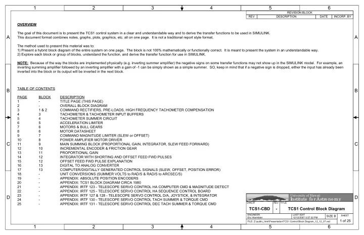
OVERVIEW The goal of this document is to present the TCS1 control system in a clear and understandable way and to derive the transfer functions to be used in SIMULINK. This document format combines notes, graphs, plots, graphics, etc. all on one page. It is not a traditional report style format. The method used to present this material was to: 1) Present a hybrid block diagram of the entire system on one page. The block is not 100% mathematically or functionally correct. It is meant to present the system in an understandable way. 2) Explore each block or group of blocks, understand the function, and derive the transfer function for use in SIMULINK. NOTE: Because of the way the blocks are implemented physically (e.g. inverting summer amplifier) the negative signs on some transfer functions may not show up in the SIMULINK model. For example, an inverting summing amplifier followed by an inverting amplifier with a gain of -1 can be simply shown as a simple summer. SO, keep in mind that if a negative sign is dropped, either the input has already been inverted into the block or its output will be inverted in the next block. TABLE OF CONTENTS PAGE BLOCK DESCRIPTION 1
- TITLE PAGE (THIS PAGE)
2
- OVERALL BLOCK DIAGRAM
3 1 & 2 COMMAND RECTIFIERS, PRE-LOADS, HIGH FREQUENCY TACHOMETER COMPENSATION 4 3 TACHOMETER & TACHOMETER INPUT BUFFERS 5 4 TACHOMETER SUMMER CIRCUIT 6 5 ACCELERATION LIMITER 7 6 MOTORS & BULL GEARS 8 6 MOTOR DATASHEET 9 7 COMMAND MAGNITUDE LIMITER (SLEW or OFFSET) 10 8 POWER AMPLIFIER MOTOR DRIVER 11 9 MAIN SUMMING BLOCK (PROPORTIONAL GAIN, INTEGRATOR, SLEW FEED FORWARD) 12 10 INCREMENTAL ENCODER & FRICTION GEAR 13 11 PROPORTIONAL GAIN 14 12 INTEGRATOR WITH SHORTING AND OFFSET FEED FWD PULSES 15 12 OFFSET FEED FWD PULSE EXPLANATION 16 13 DIGITAL TO ANALOG CONVERTER 17 13 COMPUTER/DIGITALLY GENERATED CONTROL SIGNALS (SLEW, OFFSET, POSITION ERROR) 18
- UNIT CONVERSIONS (SUMMER VOLTS to RAD/S & RAD/S to ARCSEC/S)
19
- APPENDIX: ABSOLUTE POSITION ENCODERS
20
- APPENDIX: TCS1 BLOCK DIAGRAM CIRCA 1980
21
- APPENDIX: IRTF 123 - TELESCOPE SERVO CONTROL HA COMPUTER CMD & MAGNITUDE DETECT
22
- APPENDIX: IRTF 125 - TELESCOPE SERVO CONTROL HA SEQUENCE CONTROL BOARD
23
- APPENDIX: IRTF 127 & 128 - TELESCOPE SERVO CONTROL D/A, JOYSTICK, & INTEGRATOR
24
- APPENDIX: IRTF 130 - TELESCOPE SERVO CONTROL TACH SUMMER & TORQUE CMD
25
- APPENDIX: IRTF 131 - TELESCOPE SERVO CONTROL DEC TACH SUMMER & TORQUE CMD