
SLIDE 1
1
Modern DRAM Memory Architectures
Sam Miller Tam Chantem Jon Lucas
CprE 585 Fall 2003
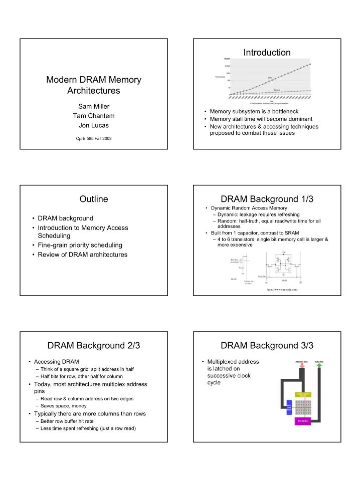
Introduction
- Memory subsystem is a bottleneck
- Memory stall time will become dominant
- New architectures & accessing techniques
proposed to combat these issues
Outline
- DRAM background
- Introduction to Memory Access
Scheduling
- Fine-grain priority scheduling
- Review of DRAM architectures
DRAM Background 1/3
- Dynamic Random Access Memory
– Dynamic: leakage requires refreshing – Random: half-truth, equal read/write time for all addresses
- Built from 1 capacitor, contrast to SRAM
– 4 to 6 transistors; single bit memory cell is larger & more expensive
http://www.cmosedu.com
DRAM Background 2/3
- Accessing DRAM
– Think of a square grid: split address in half – Half bits for row, other half for column
- Today, most architectures multiplex address
pins
– Read row & column address on two edges – Saves space, money
- Typically there are more columns than rows
– Better row buffer hit rate – Less time spent refreshing (just a row read)
DRAM Background 3/3
- Multiplexed address