
SLIDE 1
S2, 2008 COMP9032 Week5 1
Microprocessors & Interfacing
Buses and Parallel Input/Output
Lecturer : Dr. Annie Guo
S2, 2008 COMP9032 Week5 2
Lecture Overview
- Buses
– Computer buses
- I/O Addressing
– Memory mapped I/O – Separate I/O
- Parallel Input/Output
– AVR examples
S2, 2008 COMP9032 Week5 3
Five Components of Computers
Processor (active) Computer Control (“brain”) Datapath (“brawn”) Memory (passive) (where
programs, data live when running)
Devices Input Output Keyboard Mouse Disk, Display, Printer Disk
S2, 2008 COMP9032 Week5 4
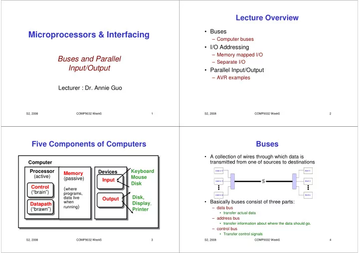
Buses
- A collection of wires through which data is
transmitted from one of sources to destinations
- Basically buses consist of three parts:
– data bus
- transfer actual data
– address bus
- transfer information about where the data should go.
– control bus
- Transfer control signals
source 1 source 2 source n dest 1 dest 2 dest n