MIPS Pipeline with Tomasulos Algorithm ADD ADD RS IR Issue WB - - PowerPoint PPT Presentation

mips pipeline with tomasulo s algorithm add add rs ir
SMART_READER_LITE
LIVE PREVIEW

MIPS Pipeline with Tomasulos Algorithm ADD ADD RS IR Issue WB - - PowerPoint PPT Presentation

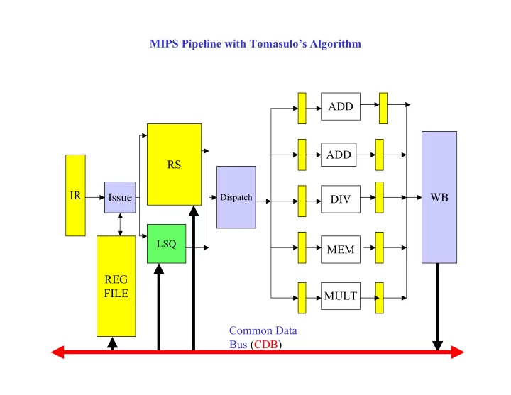
MIPS Pipeline with Tomasulos Algorithm ADD ADD RS IR Issue WB Dispatch DIV LSQ MEM REG FILE MULT Common Data Bus (CDB) Renaming Source Registers Example A: DIVD F0 , F2, F4 RAW dependency between (A,B) B: ADDD F6, F0 , F8


slide-1
SLIDE 1

MIPS Pipeline with Tomasulo’s Algorithm Issue ADD MULT DIV

LSQ

IR WB ADD RS

Dispatch

REG FILE Common Data Bus (CDB) MEM

slide-2
SLIDE 2

Renaming Source Registers

Example

A: DIVD F0, F2, F4 RAW dependency between (A,B) B: ADDD F6, F0, F8 WAR dependency between (B,C) C: SUBD F8, F10, F12 RAW dependency between (C,D) D: DIVD F0, F8, F10

  • A source register that is not the destination of an in-flight instruction is copied to the

new storage location allocated for the source operand

  • A source register that is the destination of an in-flight instruction is tagged with the id
  • f the producer
  • When the producer instruction does a write the value and its id are broadcast on

the CDB

  • The waiting instruction copies the value from the CDB to the storage allocated for

the source operand

2

slide-3
SLIDE 3

Example (Issue Unit)

Issue A: DIVD F0, F2, F4

TAG SOURCE1 SOURCE2 OP

  • v2, v4: Values read from registers F2, F4 during issue
  • Record A as the current writer of F0

RSA DIVD

v2 v4

RSA

Issue B: ADDD F6, F0, F8

ADDD

v8

  • v8: Value read from F8
  • Other operand will be result of instruction A

RSA RSB

RSA

RSB

RSB

F6 F0

3

slide-4
SLIDE 4

Example (Issue Unit)

Issue C: SUBD F8, F10, F12

TAG SOURCE1 SOURCE2 OP

v10, v12: Values read from registers F10, F12 during instruction issue

RSC SUBD

v10 v12 Issue D: DIVD F14, F8, F10

DIVD

v10

  • v10: Value read from F10
  • Other operand will be result of instruction C

RSC

RSC

RSD

RSD

RSC RSD

F14 F8

4

slide-5
SLIDE 5

Dispatch and WB Units

  • Dispatch unit selects instructions from RS whose :
  • perands are available and functional unit is free
  • In the example A, C are ready to execute.
  • When execution is complete the Write Unit is notified

Write Unit selects one of the completed instruction in EX/WB register for WB For the selected instruction, say RSI

  • Broadcast its result on the CDB
  • Broadcast the TAG (RSI) along with the value
  • All units that are waiting on the result of the completing instruction (tag

comparison): copy the broadcast value

  • Reservation stations copy the value into the RS registers with matching tags
  • Register file copies the value into the destination register of the instruction.

5

slide-6
SLIDE 6

Snapshot after Issue of A, B, C, D

Issue A: DIVD F0, F2, F4

TAG SOURCE1 SOURCE2 OP RSA DIVD

v2 v4

RSA

Issue B: ADDD F6, F0, F8

ADDD

v8 RSA RSB

RSA

RSB

RSB

F6 F0

6

TAG SOURCE1 SOURCE2 OP RSC SUBD

v10 v12 RSC

Issue D: DIVD F14, F8, F10

DIVD

v10 RSD

RSD

RSC

F14 F8

RSC

Issue C: SUBD F8, F10, F12

RSD

slide-7
SLIDE 7

Example (contd ...)

Event: C completes execution Write Unit broadcasts result (RESC) of C together with its tag RSC C releases Reservation Station RSC All registers of the RS and all registers in the Register File monitor CDB for broadcast TAG If the TAG matches copy the broadcast value into the register ID SOURCE1 SOURCE2 OP

F8

RSC SUBD

v10 v12

RESC RSD DIVD RESC

v10

RSD RSD

  • F8 updated with result of C even though B has not yet started execution.
  • A in execution
  • D ready to be dispatched

RSC F14

7

slide-8
SLIDE 8

Example (contd ...)

Event: A completes execution Write Unit broadcasts result (RESA) of A along with its tag RSA A releases RSA ID SOURCE1 SOURCE2 OP

F0

RSA DIVD

v2 v4

RESA RSB DIVD RESA

v8

RSB RSB

  • D in execution.
  • B ready to dispatch
  • When D and B complete execution, their results are broadcast and used to update F14 and

F6 respectively. RSA F6

8

slide-9
SLIDE 9

WAW Hazards

A: DIVD F0, F2, F4 B: ADDD F6, F0, F8 C: DIVD F0, F10, F12 D: ADDD F8, F0, F14

ID SOURCE1 SOURCE2 OP RSB ADDD

v8

RSB

  • Write of F0 by A effectively canceled.
  • Intermediate instructions (like B) get operands directly from A bypassing F0.

RSA DIVD

v2 v4

RSA RSC DIVD

v10 v12

RSC RSA

RSA RSB RSC

F6 F0 F0

9

slide-10
SLIDE 10

WAW Hazards

A: DIVD F0, F2, F4 B: ADDD F6, F0, F8 C: DIVD F0, F10, F12 D: ADDD F8, F0, F14

ID SOURCE1 SOURCE2 OP RSB ADDD

v8

RSB

  • Write of F0 by A effectively canceled.
  • Intermediate instructions (like B) get operands directly from A bypassing F0.

RSA DIVD

v2 v4

RSA RSC DIVD

v10 v12

RSC RSA

RSA RSB RSC

F6 F0 F0

10

slide-11
SLIDE 11

WAW Hazards

A: DIVD F0, F2, F4 B: ADDD F6, F0, F8 C: DIVD F0, F10, F12 D: ADDD F8, F0, F14

ID SOURCE1 SOURCE2 OP RSB ADDD

v8

RSB

  • Write of F0 by A effectively canceled.
  • Intermediate instructions (like B) get operands directly from A bypassing F0.

RSA DIVD

v2 v4

RSC DIVD

v10 v12

RSC RSA

RSA RSB RSC

F0 F6 F0

RSD

F8 RSC RSD ADDD

v14

RSB RSD

RSD

11

slide-12
SLIDE 12

Load Store Queue (LSQ)

LOAD/STORE BUFFERS FIFO QUEUE

CDB

MEM DISPATCH ISSUE WRITE

  • In-flight LOAD or STORE instructions are held in Load/Store Buffers in the LSQ unit
  • LOAD dispatched to memory when MEM is free
  • STORE dispatched when MEM is free and value to be stored is available in the Load/Store Buffer
  • STORE value either copied from REG during issue or copied from CDB while waiting
  • We will assume that the effective address is calculated during the ISSUE stage

LSQ

12

slide-13
SLIDE 13

Load Store Queue (LSQ)

LSQ: FIFO Queue that holds descriptors of issued LOAD and STORE instructions LOAD and STORE instructions wait in LSQ for memory access. ID MEM ADDR OPERAND OP

LSQA SD ea

LSQA LSQB LSQ Buffers ID: Identifies buffer (which also serves as the identification of the issued instruction) OP: Load or Store (may be implicit if the queues for LOAD and STORE are separate) MEM ADDR: Holds the effective address of the memory location to be accessed OPERAND: (STORE only) Holds value to be stored in memory When a SD instruction is issued the Buffer may either receive the:

  • Actual operand value by copying it from the source register or
  • Tag of the instruction producing the value if it (producer instruction) is still in flight

ID MEM ADDR OP

LSQB ea LD

13

slide-14
SLIDE 14

Load/Store Buffers

Load and Store Buffers: Hold descriptors for Load and Store instructions A: SD 0(R1), F0 I: ADDD F0, F2, F4 B: LD 0(R2), F2 A: SD 0(R1), F0 B: LD 0(R2), F2 ID ADDRESS OPERAND OP

SQA SD

ea v0

LQB LD ea F2 LQB SQA LQB SQA SD

ea RSI

SQA ea ea

14

slide-15
SLIDE 15

Example Schedule

LOOP: A LD F0, 0(R1) | temp = x[i] B MUL F4, F0, F2 | temp = temp * a C SD F4, 0(R1) | x[i] = temp D ADDI R1, R1, #8 | i++ E BNE R1, R2, LOOP | branch if R1.ne.R2

  • Within an iteration RAW between (A, B) and (C, D) [focusing on FP registers only]
  • Across iterations WAR and WAW dependencies become apparent

A1 LD F0, 0(R1) B1 MUL F4, F0, F2 C1 SD F4, 0(R1) D1 ADDI R1, R1, #8 E1 BNE R1, R2, LOOP A2 LD F0, 0(R1) WAR with B1, WAW with A1 B2 MUL F4, F0, F2 WAR with C1, WAW with B1 C2 SD F4, 0(R1) D2 ADDI R1, R1, #8 E2 BNE R1, R2, LOOP

15

slide-16
SLIDE 16

Assumptions in Constructing Schedule

  • MUL unit is 4 cycles fully pipelined
  • There are an unlimited number of buffers in LSQ
  • Hence we never stall ISSUE for want of a buffer in the LSQ unit
  • Assume that Branches are predicted as Taken
  • The Target Address is calculated during the ISSUE stage of the Branch
  • Hence there is a 1 cycle stall between the issue of the Branch instruction and the issue of the

instruction at the target address

  • When a LD or SD instruction is issued the effective memory address is calculated in the Issue stage
  • That is, the base address register Rn is read and the offset added to it
  • The effective address is put into the appropriate field of the Buffer in the LSQ
  • The integer ALU instructions do not go through the FP or MEM pipeline
  • They read the source registers in the ID stage
  • Execute at the next cycle in the EX stage
  • Write on the following cycle to the integer register
  • Forwarding is assumed to be used whenever beneficial to reduce latency of integer instructions

16

slide-17
SLIDE 17

Example Schedule

LOOP: | Assume R1 = 1000 initially; Assume F2 = 200 A1 LD F0, 0(R1) | temp = x[i] B1 MUL F4, F0, F2 | temp = temp * a C1 SD F4, 0(R1) | x[i] = temp D1 ADDI R1, R1, #4 | Index next element of the array E1 BNE R1, R2, LOOP | branch if R1.ne.R2 R2 is the address past end of array Cycle 2. Issue A1

F0 LD LQA1

&x[0] = 1000

Cycle 3. Issue B1

F4

RSB1

MUL RSB1 v2= 200

LQA

LQA1

Cycle 4. Issue C1

SD SQC1

RSB1

LQA1

r1 &x[0] = 1000

v2 = 200

17

slide-18
SLIDE 18

Schedule

21 20 E2 D2 C2 B2 A2 E1

IF

D1

I IF

C1

D I IF

B1

M D I IF

A1 19 18 17 16 15 14 13 12 11 10 9 8 7 6 5 4 3 2 1 Cycle 4: A1: Memory Read B1: In RS in Dispatch stage C1: In I stage. Will issued to LOAD Buffer at end of cycle

  • Effective Address &x[0] = 1000 and tag LQC

18

slide-19
SLIDE 19

Example Schedule

Cycle 3 A: in D stage. Ready to be dispatched to MEM B: in I stage. Will issue to RS at end of cycle Cycle 4 A: Memory Read B: Waiting in RS since operand not yet available C: In I stage. Will issued to LOAD Buffer at end of cycle

  • Effective Address &x[0] = 1000 and tag LQC

Cycle 5 A: In WRITE stage. WRITE unit broadcasts value read from memory (i.e x[0] value) along with tag LQA B: Finds a match between the broadcast tag LQA and copies broadcast data value into the RS field C: Waiting in LSQ since operand F4 not yet available. Requires MUL to produce the value. D: Integer instruction issued (reads register R1) Cycle 6 B: All operands available; MUL unit free. Dispatched from the RS to the MUL unit C: Still waiting for the MUL value to be broadcast D: ADDI instruction in integer EX stage E: Branch instruction in Issue Stage. Calculates effective address (that of LOOP) and will put the address into PC at the end of the cycle Cycle 7 B: Second cycle of MUL C: Still waiting for the MUL value to be broadcast D: ADDI instruction writes updated R1 (1004) E: Branch instruction in EX Stage. Compares registers and finds its prediction is correct A2: Second iteration begins in IF stage.

19

slide-20
SLIDE 20

Schedule

21 20 E2 D2 C2 B2 A2

IF

E1

I IF

D1

D I IF

C1

D D I IF

B1

W M D I IF

A1 19 18 17 16 15 14 13 12 11 10 9 8 7 6 5 4 3 2 1 Cycle 5 A: In WB stage. WB unit broadcasts value read from memory (i.e x[0] value) along with tag LQA1 B: Finds a match between the broadcast tag LQA and copies broadcast data value into the RS field C: Waiting in LSQ since operand F4 not yet available. Requires MUL to produce the value. D: Integer instruction issued (reads register R1)

20

slide-21
SLIDE 21

Example Schedule

Cycle 5. WB broadcasts value of x[0] along with TAG LQA1 F0 and RSB1 copy the broadcast value. LOAD buffer held by instruction A1 is released

FO: x[0]

RSB1

MUL RSB1 v2 = 200 SD SQC1 &x[0]

RSB1

x[0] F4 LQA

1

21

slide-22
SLIDE 22

E2 D2 C2 B2

IF

A2

I IF

E1

E I IF

D1

D D I IF

C1

* D D I IF

B1

W M D I IF

A1 6 5 4 3 2 1 Cycle 6: B1: All operands available; MUL unit is free. So B is begins execution in the MUL unit D1: ADDI instruction in integer EX stage E1: Branch instruction in Issue Stage. Calculates effective address (that of LOOP) and will put the address into PC at clock edge

22

slide-23
SLIDE 23

21 20 E2 D2 C2 B2

IF

A2

E I IF

E1

W E I IF

D1

D D D I IF

C1

* * D D I IF

B1

W M D I IF

A1 19 18 17 16 15 14 13 12 11 10 9 8 7 6 5 4 3 2 1

Cycle 7 B1: Second cycle of MUL C: Still waiting for the MUL value to be broadcast D1: ADDI instruction writes updated R1 (1004) E1: Branch instruction in EX Stage. Compares registers and finds its prediction is correct A2: Second iteration begins in IF stage. 23

slide-24
SLIDE 24

Example Schedule

F0 LD LQA2 &x[1]

Cycle 9. Issue B2

F4

RSB2

MUL RSB2 v2 = 200

LQA2

Cycle 10. Issue C2

SD SQC2

RSB2

LQA2

Cycle 8. Issue A2

&x[1] Instructions issued during iteration 2 denoted by A2, B2, C2 etc

24

slide-25
SLIDE 25

Schedule

21 20 E2 D2

IF

C2

I IF

B2

D I IF

A2

W E I IF

E1

W E I IF

D1

D D D D D I IF

C1

* * * * D D I IF

B1

W M D I IF

A1 19 18 17 16 15 14 13 12 11 10 9 8 7 6 5 4 3 2 1

25

slide-26
SLIDE 26

Snapshot of RS and LSQ Buffers at Cycle 10

LD LQA2 &x[1] = 1004 F4 MUL RSB2 v2 = 200

LQA2

SD SQC2

RSB2

LQA2

&x[1] = 1004 FO: x[0] MUL v2 = 200 SD SQC1 &x[0] = 1000 RSB1 x[0]

LQA

F0: x[0]

RSB1

F4 RSB1

RSB2

F4 was to be written with the result of B. However when C2 was issued this write was CANCELLED. That is B2 became the new writer for F4. Canceling the write of F4 by B is not a problem . Why? C which wants that value will get it directly from the CDB when the WB unit broadcasts the value along with the tag RSB

26

slide-27
SLIDE 27

Schedule

/

21 20 E2

IF

D2

I IF

C2

D I IF

B2

D D I IF

A2

W E I IF

E1

W E I IF

D1

D D D D D D I IF

C1

W * * * * D D I IF

B1

W M D I IF

A1 19 18 17 16 15 14 13 12 11 10 9 8 7 6 5 4 3 2 1

27

NOTE: LD of A2 at cycle 10 has stalled for earlier SD (of C1) since we assume LSQ dispatches requests in strict FIFO order.

slide-28
SLIDE 28

Schedule

/

21 20

IF

E2

I IF

D2

D I IF

C2

D D I IF

B2

D D D I IF

A2

W E I IF

E1

W E I IF

D1

M D D D D D D I IF

C1

W * * * * D D I IF

B1

W M D I IF

A1 19 18 17 16 15 14 13 12 11 10 9 8 7 6 5 4 3 2 1

27

NOTE: LD of A2 at cycle 11 still stalled for earlier SD (of C1) since we assume LSQ dispatches requests in strict FIFO order.

slide-29
SLIDE 29

Schedule

/

21 20

I IF

E2

E I IF

D2

D D I IF

C2

D D D I IF

B2

M D D D I IF

A2

W E I IF

E1

W E I IF

D1

M D D D D D D I IF

C1

W * * * * D D I IF

B1

W M D I IF

A1 19 18 17 16 15 14 13 12 11 10 9 8 7 6 5 4 3 2 1

27

NOTE: LD of A2 at cycle 10 has stalled for earlier SD (of C1) since we assume LSQ dispatches requests in strict FIFO order.

slide-30
SLIDE 30

Schedule

/

W

21

M

20

D D D D D I IF

A3

W E I IF

E2

W E I IF

D2

M D D D D D D D D I IF

C2

W * * * * D D D D I IF

B2

W M D D D I IF

A2

W E I IF

E1

W E I IF

D1

M D D D D D D I IF

C1

W * * * * D D I IF

B1

W M D I IF

A1 19 18 17 16 15 14 13 12 11 10 9 8 7 6 5 4 3 2 1

27

NOTE: Completes SD every 8 cycles apart 8(n-1) + 11 = 8n +3 cycles. Additional stalls will arise as RS fills up

slide-31
SLIDE 31

Schedule

/

21 20 E2

IF

D2

I IF

C2

D I IF

B2

M D I IF

A2

W E I IF

E1

W E I IF

D1

D D D D D D I IF

C1

W * * * * D D I IF

B1

W M D I IF

A1 19 18 17 16 15 14 13 12 11 10 9 8 7 6 5 4 3 2 1

27

WARNING: In the schedule above M stage (LD) of A2 at cycle 10 has overtaken earlier SD (of C1). Not valid if LSQ dispatches requests in strict FIFO order.

slide-32
SLIDE 32

Schedule

21 20

IF

E2

I IF

D2

D I IF

C2

D D I IF

B2

W M D I IF

A2

W E I IF

E1

W E I IF

D1

M D D D D D D I IF

C1

W * * * * D D I IF

B1

W M D I IF

A1 19 18 17 16 15 14 13 12 11 10 9 8 7 6 5 4 3 2 1 T = 6(n-1) + 11 = 6n + 5 cycles for n iterations

28

slide-33
SLIDE 33

Schedule

21 20

IF

E2

I IF

D2

D I IF

C2

D D I IF

B2

W M D I IF

A2

W E I IF

E1

W E I IF

D1

M D D D D D D I IF

C1

W * * * * D D I IF

B1

W M D I IF

A1 19 18 17 16 15 14 13 12 11 10 9 8 7 6 5 4 3 2 1 T = 6(n-1) + 11 = 6n + 5 cycles for n iterations

28

slide-34
SLIDE 34

Schedule

21 20

I IF

E2

E I IF

D2

D D I IF

C2 *

D D I IF

B2

W M D I IF

A2

W E I IF

E1

W E I IF

D1

M D D D D D D I IF

C1

W * * * * D D I IF

B1

W M D I IF

A1 19 18 17 16 15 14 13 12 11 10 9 8 7 6 5 4 3 2 1 T = 6(n-1) + 11 = 6n + 5 cycles for n iterations

29

slide-35
SLIDE 35

Schedule

21 20

W M D I IF W E I IF

E2

W E I IF

D2

M D D D D D D I IF

C2 W * * * *

D D I IF

B2

W M D I IF

A2

W E I IF

E1

W E I IF

D1

M D D D D D D I IF

C1

W * * * * D D I IF

B1

W M D I IF

A1 19 18 17 16 15 14 13 12 11 10 9 8 7 6 5 4 3 2 1 T = 6(n-1) + 11 = 6n + 5 cycles for n iterations

30