Scaling and Technology Issues for Soft Error Rates Allan. H. - - PDF document

scaling and technology issues for soft error rates
SMART_READER_LITE
LIVE PREVIEW

Scaling and Technology Issues for Soft Error Rates Allan. H. - - PDF document

Presented at the 4th Annual Research Conference on Reliability, Stanford University, October 2000 Scaling and Technology Issues for Soft Error Rates Allan. H. Johnston Jet Propulsion Laboratory California Institute of Technology Pasadena,


slide-1
SLIDE 1

Presented at the 4th Annual Research Conference on Reliability, Stanford University, October 2000

1

Scaling and Technology Issues for Soft Error Rates

  • Allan. H. Johnston

Jet Propulsion Laboratory California Institute of Technology Pasadena, California

Abstract - The effects of device technology and scaling on soft error rates are discussed, using information obtained from both the device and space communities as a guide to determine the net effect on soft errors. Recent data on upset from high- energy protons indicates that the soft-error problem in DRAMs and microprocessors is less severe for highly scaled devices, in contrast to expectations. Possible improvements in soft-error rate for future devices, manufactured with silicon-on-insulator technology, are also discussed.

  • I. INTRODUCTION

Soft-errors from alpha particles were first reported by May and Woods [1], and considerable effort was spent by the semiconductor device community during the ensuing years to deal with the problem of errors from alpha particles in packaging, metallization and other materials. This included modifications in device design to reduce the inherent sensitivity to extraneous charge, as well as application of topical shielding and improvements in material purity. Atmospheric neutrons can also produce soft errors. One example is shown in Figure 1, after Lage, et al.[2], which shows the increase in measured soft error rate when experiments were done on SRAMs using alpha sources with different intensities. The increased error rate is due to the presence of atmospheric neutrons that have a larger relative influence when alpha experiments are done for long time periods using low-intensity sources.

Figure 1. Increase in soft-error rate of an SRAM when low- intensity alpha particle sources are used.

  • - - - - - -

The research in this paper was carried out by the Jet Propulsion Laboratory, California Institute of Technology, under contract with the National Aeronautics and Space Adminstration (NASA) under the NASA Electronics Parts and Packaging Program (ERC).

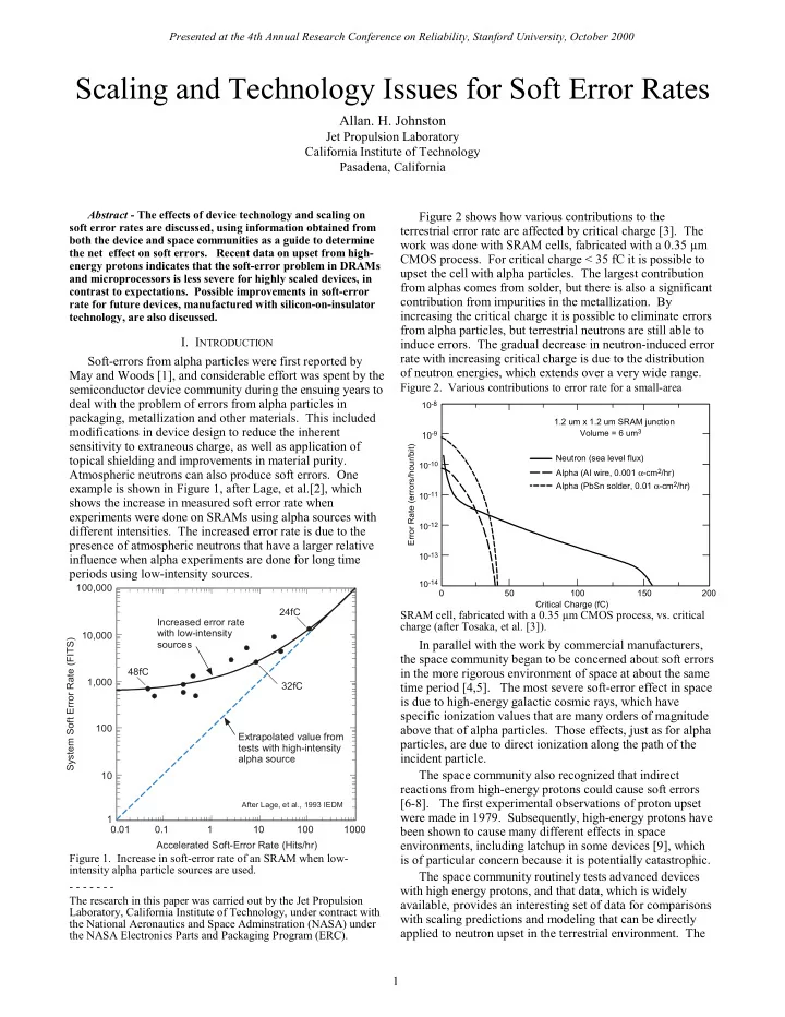
Figure 2 shows how various contributions to the terrestrial error rate are affected by critical charge [3]. The work was done with SRAM cells, fabricated with a 0.35 µm CMOS process. For critical charge < 35 fC it is possible to upset the cell with alpha particles. The largest contribution from alphas comes from solder, but there is also a significant contribution from impurities in the metallization. By increasing the critical charge it is possible to eliminate errors from alpha particles, but terrestrial neutrons are still able to induce errors. The gradual decrease in neutron-induced error rate with increasing critical charge is due to the distribution

  • f neutron energies, which extends over a very wide range.

Figure 2. Various contributions to error rate for a small-area SRAM cell, fabricated with a 0.35 µm CMOS process, vs. critical charge (after Tosaka, et al. [3]).

In parallel with the work by commercial manufacturers, the space community began to be concerned about soft errors in the more rigorous environment of space at about the same time period [4,5]. The most severe soft-error effect in space is due to high-energy galactic cosmic rays, which have specific ionization values that are many orders of magnitude above that of alpha particles. Those effects, just as for alpha particles, are due to direct ionization along the path of the incident particle. The space community also recognized that indirect reactions from high-energy protons could cause soft errors [6-8]. The first experimental observations of proton upset were made in 1979. Subsequently, high-energy protons have been shown to cause many different effects in space environments, including latchup in some devices [9], which is of particular concern because it is potentially catastrophic. The space community routinely tests advanced devices with high energy protons, and that data, which is widely available, provides an interesting set of data for comparisons with scaling predictions and modeling that can be directly applied to neutron upset in the terrestrial environment. The

10-14 1.2 um x 1.2 um SRAM junction 50 100 150 200 10-13 10-12 10-11 10-10 10-9 10-8 Neutron (sea level flux) Alpha (AI wire, 0.001 α-cm2/hr) Alpha (PbSn solder, 0.01 α-cm2/hr) Volume = 6 um3 Error Rate (errors/hour/bit) Critical Charge (fC)

1000 100,000 System Soft Error Rate (FITS) 10,000 1,000 100 10 1 0.1 0.01 1 10 100 Increased error rate with low-intensity sources Extrapolated value from tests with high-intensity alpha source 48fC 32fC 24fC Accelerated Soft-Error Rate (Hits/hr)

After Lage, et al., 1993 IEDM

slide-2
SLIDE 2

Presented at the 4th Annual Research Conference on Reliability, Stanford University, October 2000

2 space community also routinely tests devices with heavy

  • ions. For example, Figure 3 shows how the cross sections of

internal registers and cache memory of a microprocessor increase when tests are done with long-range ions that have different values of LET. (For reference, the LET of a 5-MeV alpha particle is 1 MeV-cm2/mg). The heavy-ion data provides a direct indication of the specific ionization track density required for upset, and is a useful way to compare the upset sensitivity of different devices.

Figure 3. Dependence of cross section on linear energy transfer for a microprocessor. The upset threshold is slightly above the LET for a 5-MeV alpha particle.

  • II. SPACE AND TERRESTRIAL ENVIRONMENTS
  • A. Comparison of Environments

The high-energy cosmic rays that spacecraft encounter are largely shielded by the earth’s atmosphere. Consequently they do not occur in significant numbers in terrestrial

  • applications. However, the interaction of cosmic rays in the

upper atmosphere produces secondary particles, including

  • neutrons. The neutrons have a low interaction probability

with the atmosphere, and significant numbers of energetic neutrons arrive at the earth’s surface. Although spacecraft are usually not concerned with neutrons, most space environments include high-energy protons with a wide distribution of energies. Direct ionization from protons is generally too low to be of concern in microelectronics. However, protons can produce nuclear reactions in silicon, and the secondary reaction products from reactions or nuclear collisions -- which have relatively short range -- produce ionization tracks with much higher charge densities compared to those generated along the path of the high-energy protons that initiate the reaction. However, the cross section for such indirect processes is much smaller than for direct ionization because the incoming particle has to undergo a nuclear collision in order to produce the reaction (nuclear cross sections are typically 10-4 to 10-5 lower). Protons with energies above 50 MeV have cross sections for nuclear reactions that are nearly identical to those for high-energy neutrons. This allows test results for high- energy protons to be extended directly to neutron environments, which has been noted by workers in both the semiconductor and space environments [10,11]. The proposed standard for evaluating SER rates in terrestrial applications allows protons to be used as an alternative to tests with neutron sources [12]. Although cross sections for protons and neutrons are nearly the same at high energies, that is not the case for lower energies (<50 MeV). At low energies, protons cross sections increase because of Coulomb interactions with the lattice atoms, causing the cross section to increase with decreasing energy. In addition, the neutron energy distribution of the uncharged neutrons in terrestrial environments extends to much lower energies than the distribution of protons within spacecraft because even moderate amounts of shielding eliminate most of the low-energy protons in space. Figure 4 compares the distribution of atmospheric neutrons (actually the energy distribution of the white neutron source at Los Alamos National Laboratory) with the typical distribution of proton energies in spacecraft.

Figure 4. Energy distributions of atmospheric neutrons on the ground and protons in an earth-orbiting spacecraft.

The point of this figure is to show that the proton spectrum in space decreases at low energies, reducing the importance (and interest) of low energy protons in causing errors in spacecraft. On the other hand, the relative number

  • f neutrons in terrestrial environments continues to increase

at low energies. Thus, the soft-error rate problem on the ground is much more affected by reductions in the threshold energy for errors from neutron-induced reactions compared to the soft-error problem in space (from protons).

  • B. Recoil Energy Distribution

A great deal of experimental work has been done to investigate the distribution of recoil energies when experiments are done with monoenergetic protons [13,14]. That work has shown that there is a continuous distribution

  • f recoil energies that decreases up to a maximum energy.

For silicon, the maximum recoil energy due to elastic collisions is 13.6% of the energy of the incident particle. This means that for 100 MeV protons (or neutrons), the

Cross Section (cm2/bit) LET (MeV-cm2/mg) 10-8 10 20 30 40 10-7 10-6 10-5 10-4 10-3 10-2 10-1 10-10 10-9 Dynamic Test (Cache Enabled) Registers 10-2 D i f f e r e n t i a l F l u x ( p a r t i c l e s / c m

2-

s e c

  • M

e V ) Neutron or Proton Energy, MeV 10 1000 1 10-3 10-4 10-5 10-6 100 10-7 109 108 107 106 105 104 protons neutrons

slide-3
SLIDE 3

Presented at the 4th Annual Research Conference on Reliability, Stanford University, October 2000

3 maximum total energy of a recoil is 13.6 MeV. However, there are very few particles with maximum recoil energy. The energy distribution decreases roughly as 1/E up to the maximum recoil energy. The range of the recoil products varies with energy. For the case where the incident particle energy is 100 MeV the more energetic recoils have ranges up to 5 µm, but most of the particles have ranges below 2 µm. For the real environments in terrestrial or space environments the net distribution of recoils is a superposition

  • f the distribution of energetic primary particles along with

the energy distribution of the recoil products. Most of the recoils will have relatively short ranges, but “short” is a relative term. For older technologies, one could make the assumption that the entire recoil energy was absorbed within the sensitive volume of a sensitive device because device dimensions were considerably larger than the range of most

  • recoils. That is no longer true for highly scaled devices,

which affects the collected charge.

  • C. Effective Volume for Recoil Products

Many of the recoil products have ranges that are considerably longer than the average charge collection depth. Thus, particles that undergo collisions outside the charge collection region may have sufficient energy to reach the sensitive region and deposit part of the energy in that region. One way to deal with this is to define a generation rate for recoils (referred to as the burst generation rate) and then assume an extended region outside the charge collection region for the total sensitive volume [15-18]. This approach has been reasonably effective for older generation devices, but needs to be modified to handle modern devices with smaller sensitive volumes [ref]. It is also important to realize that the charge collection region is not really constant, but changes dimensions depending on the total deposited energy and location because the depletion region collapses if the energy is sufficiently high. Charge collection volumes for DRAMs are quite complex because diffused charge in the substrate, well beyond the depletion region, can be collected by a reverse-biased

  • junction. Figure 5 shows the results of calculations of the

charge collected by particles that produce charge tracks well away from the depletion region [19] (similar to the situation in the bulk substrate of a DRAM). These calculations were done with the PISCES device analysis program. Note that nearly all of the deposited charge is collected, but the time

  • ver which the charge collection occurs extends to relatively

long time intervals. For DRAMs this is an important effect because the charge will be effective in fully or partially discharging the storage capacitor. Although the same charge collection process will take place in SRAMs or logic devices, they are generally only sensitive to charge collected in short time periods, unlike DRAMs. Thus, charge collection depends not only on substrate properties, but also on the way in which the circuit responds to longer duration charge pulses.

Figure 5. Charge collection from short range recoils at various distances from the depletion region of a p-n junction.

  • III. DEVICE SCALING TRENDS
  • A. Scaling for Microprocessors and Logic

Device scaling is an extremely complex topic that involves many assumptions about technology evolution. The earliest studies were done by Dennard, et al. at IBM [20]. More recent studies by Davari, et al. [21] and Hu [22] have discussed scaling trends for two basic technology directions: high performance, where power dissipation is a secondary concern; and low power, where power and performance are both considered. Table 1, after Davari, presents the results based on the state-of-the-art in 1995. Those predictions have been reasonably accurate in predicting future technology

  • trends. For radiation susceptibility, the key parameters are

gate oxide thickness, relative speed and density, and power supply voltage which affect charge collection and critical charge.

Table 1. Scaling Predictions for High-Performance and Low- Power Logic Circuits (after Davari, et al. [21])

  • B. Scaling for Memories

Memory technologies involve quite different scaling

  • assumptions. There are two reasons for this: first, memory

technologies require very low leakage and hence must impose a much higher ratio between “on” and “off” transistors within the memory; and second, memories are generally sold at very low prices compared to microprocessors and other high-performance devices, resulting in much more conservative approaches for device design.

Supply voltage (V) High performance Low power

  • Lithog. resolution (µm)

Channel length (µm) Gate oxide thickness (nm) Relative density Relative speed High performance Low power Parameter 5

  • 1.25

0.9 23 1.0 1.0

  • Late

1980's 5/3.3 3.3/2.5 0.8 0.6/0.45 15/12 2.5 1.4/2.0 1.0/1.6 1992 3.3/2.5 2.5/1.5 0.5 0.35/0.25 9/7 6.3 2.7/3.4 2.0/2.4 1995 2.5/1.8 1.5/1.2 0.35 0.2/0.15 6/5 12.8 4.2/5.1 3.2/3.5 1998 1.5 1.0 0.25 0.1 3.5 25 7.2 4.5 2001 1.2 1.0 0.18 0.07 2.5 48 9.6 7.2 2004

1.2 N

  • r

m a l i z e d C h a r g e 2 Distance from Top Surface (µm) 0.6 0.4 0.2 4 6 8 10 12 14 16 18 20 0.8 1.0 3.5 µm track length p-substrate: 1 x 1015 cm-3 80 ns 40 ns 20 ns 10 ns 1 ns Depletion width

slide-4
SLIDE 4

Presented at the 4th Annual Research Conference on Reliability, Stanford University, October 2000

4 There have been many changes in memory technology. For DRAMs, storage capacitor technology is one factor that has continually evolved. Although it is not possible to cover all aspects of DRAM scaling in this paper, Figure 6, after Itoh, et al. [23] shows how cell area and storage capacitor size have changed over several DRAM generations. Device dimensions have scaled inversely with memory size, as expected from general scaling trends. On the other hand, storage capacitance has decreased far more slowly. One reason for this is the need to keep the total stored charge above the charge generated by alpha particles, as well as

  • ther noise sources. The charge generated by a 5-MeV alpha

particle in one micrometer of path length is indicated on this figure for comparison. This trend in storage capacitance affects soft-error rates for proton or neutron reactions because it establishes a “floor” for charge generation.

Figure 6. Cell area and stored charge for DRAMs over several generations (after Itoh, et al. [23]).

  • C. Scaling Implications for SER Sensitivity

Charge Collection Depth The depth over which charge from a long-range ion is collected generally decreases with scaling. This is due to several factors, including the decrease in active layer thickness and increase in channel doping, which reduces the depletion width as well as charge funneling. Substrate properties also affect charge collection depth, particularly for epitaxial CMOS. Present state-of-the-art CMOS devices use epitaxial layers that are approximately 2 µm thick, effectively limiting charge collection to that region. That is not true for bulk substrates (which are typically used for memories), and thus the charge collection depth for memories can be up to an order of magnitude higher. As discussed later, circuits designed with SOI technology will further reduce charge collection depth, potentially reducing SER sensitivity by up to an order of magnitude. Switching Amplitude Power supply voltage (and total switching amplitude) directly affect critical charge and upset sensitivity. For logic circuits and SRAMs, the decrease in switching voltage reduces the voltage swing, directly affecting critical charge. That factor, along with the decease in device dimensions and increase in switching speed, will compete with the decrease in charge collection depth. For DRAMs the effect of internal voltage is less apparent because of the effect of charge leakage, which reduces the internal cell voltage between successive refresh cycles. DRAM architecture is also a factor. Most DRAMs use boosted word lines, and the internal noise margin is affected by the ratio of the bit line capacitance and the cell storage

  • capacitance. Changes in DRAM architecture have resulted

in block-oriented designs that have allowed the capacitance ratio to increase for scaled devices [24]. Architecture and device design play a large role in determining DRAM sensitivity, and make it difficult to establish general scaling trends. Critical Charge The effects of device scaling on soft-error rate depend on several competing factors. The critical charge required to upset a memory element (or active transistor) is expected to decrease with scaling. but this is partially offset by the decrease in charge collection depth as well as by device

  • architecture. Although earlier studies predicted a steady

decrease in critical charge with scaling [25], the complex interaction of device design with other scaling issues was not taken into account. Even though critical charge is expected to decrease with scaling, the net effect on threshold conditions is less obvious, and may actually improve with scaling as discussed in the next section. Designs that take upset from alpha particles into account will reduce the critical charge compared to earlier projections. Cross Sectional Area Finally, even if the first two factors cancel the decrease in device area that results from scaling will lower the total cross section per bit. Thus, the net upset rate per bit is expected to decrease with scaling even if the minimum ionization track charge density is unchanged. Other factors must also be considered. For example, devices with complex internal architectures (e.g., special internal test modes in DRAMs) may allow new types of errors to be introduced that are difficult to identify and may interfere with standard ways to detect and correct errors. The total functional capability of VLSI devices continues to increase with scaling, and thus the probability of an error within a chip may increase substantially even if the error rate per bit decreases. This has certainly been an issue in the space environment.

  • IV. TEST RESULTS FROM THE SPACE COMMUNITY
  • A. Microprocessors

Extensive work has been done on microprocessor testing during the last 15 years. That work has shown that the dominant effect of heavy ions and protons on microprocessors is upset in internal registers. Upset in random logic has not been a significant factor up to now, although this may change as microprocessors continue to evolve.

Cell Area (µm2) Memory Capacity (bit) 1 16K 256K 10 10,000 LET of 5 MeV Alpha Particle is 10 fC/µm 100 1000 1000 100 10 4M 64M 1G Cell Area Planar Trench Stack Signal Charge Qs Signal Charge Qs (fC)

slide-5
SLIDE 5

Presented at the 4th Annual Research Conference on Reliability, Stanford University, October 2000

5 One result which was certainly unexpected is that the threshold LET required to upset registers in NMOS and CMOS microprocessors has essentially not changed during the last fifteen years [26]. As shown in Table 2, the feature size used in manufacturing these devices has changed by more than one order of magnitude during that time period. The last entry in this table is for a very high speed modern microprocessor, the Power PC750. This may be influenced by overall concerns about alpha particle sensitivity by microprocessor manufacturers.

Table 2. Threshold LET for Microprocessors

It is also useful to examine trends in proton upset for

  • microprocessors. Figure 7 shows the dependence of proton

upset cross section on proton energy for register errors, normalized per bit, for two relatively advanced processors. The threshold energy is essentially the same, but the cross section of the newer Power PC750 processor is more than an

  • rder of magnitude lower than that of the older PC603e.

Both processors use thin epitaxial layers over highly doped

  • substrates. The PC603e was designed with a feature size of

0.35 µm, while the feature size of the Power PC750 was 0.25 µm. The fact that the threshold energy is approximately the same is consistent with the results in Table 2 showing nearly the same threshold LET for the two processors. However, there is an important consideration for proton recoils beyond that of threshold LET for long-range particles. As devices become smaller, the range of the recoil atoms from indirect processes increases relative to device feature size. This allows reaction products with lower energy to upset the device, potentially increasing the upset rate in the terrestrial neutron environment.

Figure 7. Comparison of proton upset for registers in high- performance microprocessors from one manufacturer that represent 1996 and 1999 design technologies.

These results are indicative of mainstream microprocessors that are fabricated on epitaxial substrates. The newer Power PC750 operates at very high clock frequencies (700 MHz). Test results on both types of processors indicate that their responses to both protons and heavy ions are dominated by errors in registers and the cache

  • memory. It is possible that faster devices may be susceptible

to transient errors in logic or other regions of the processor, creating a scenario where the upset rate may increase with further scaling. That topic is currently under investigation at JPL using next-generation microprocessors as a vehicle for

  • study. Once that threshold is reached, it may become quite

difficult to use devices in space. The error rate in the terrestrial environment will also increase, but will be of less importance because the particle flux is so much lower for the terrestrial environments.

  • B. DRAMs

Trends in DRAM responses are also of great interest. However, two points must be kept in mind: first, DRAM scaling involves very different assumptions about device parameters; and second, DRAMs are almost always fabricated on bulk substrates and are sensitive to charge collection over far longer distances. The latter factor is highly significant when comparing upset from heavy ions (with long range) and the short-range recoil products from proton or neutron reactions. Figure 8 shows how the sensitivity of proton upset rates have changed as DRAMs have evolved. The upset rate has steadily declined, on average over several DRAM

  • generations. This figure does not consider any of the details

involving the structure of individual devices, and it is apparent that there are large differences in the upset rate of devices from different manufacturers. This is probably related to the design of the wells; most DRAMs use a triple- well structure in order to reduce leakage current in the memory array.

Z-80 Zilog 1986 3 µm 1.5 - 2.5 8086 Intel 1986 1.5 µm 1.5 - 2.5 80386 Intel 1991 0.8 µm 2 - 3 68020 Mot. 1992 0.8 µm 1.5 - 2.5 LS64811 LSI 1993 1.2 µm 2 - 2.5 90C601 MHS 1993 1.2 µm 2 - 2.5 80386 Intel 1996 0.6 µm 2 - 3 PC603e Mot. 1997 0.4 µm 1.7 - 3 Pentium Intel 1997 0.35 µm 2 - 3 Power PC750 Mot. 2000 0.25 µm 2 - 2.5 Feature Threshold LET Device Manuf. Year Size (approx.)

(MeV-cm2/mg)

Cross Section (cm2/bit) Proton Energy (MeV) 100 10-12 10-13 10-14 10-15 200 300 400 PC603e Power PC 750

slide-6
SLIDE 6

Presented at the 4th Annual Research Conference on Reliability, Stanford University, October 2000

6

Figure 8. DRAM upset rate from high energy protons for various generations.

Heavy-ion results have shown that the threshold LET for DRAMs has remained between 1 and 2 MeV-cm2/mg for an extended period. In this case, the threshold is almost certainly related to concerns about alpha-particle sensitivity, which involves relatively long-range particles with LET values that are slightly below 1 MeV-cm2/mg.. Although earlier generation devices often used internal die coatings to reduce sensitivity to upset from those sources, newer generation DRAMs have taken alpha particle sensitivity into account as part of the design process [24].

  • V. PREDICTIONS FOR MORE ADVANCED TECHNOLOGIES
  • A. High-Speed/Low-Voltage Designs

As discussed earlier, one of the major concerns about high-speed devices is sensitivity to upset from internal transients in logic circuits. Clocked logic circuitry generally reduces sensitivity to such transients because the timing window is limited to periods when the clock is undergoing a logic transition. However, as devices are pushed to higher and higher speeds the relative size of the sensitive timing window increases. Reduced switching voltages increase

  • verall sensitivity to this type of error, particularly when

power dissipation is reduced. Recent simulations and models by Shin, et al. have shown how charge collected from alpha particles in very small devices is affected by junction area and switching voltage [27]. Figure 9 shows the results of those calculations, which are done for a triple-well structure in an advanced DRAM. The collected charge does not change nearly as rapidly with junction area as one would expect. This is mainly due to the collapse of internal electric fields during the first 200-500 ps

  • f the ion strike. The collapse of the field extends the charge

collection region beyond the boundaries established by the depletion region. As shown in the figure, the collected charge falls slightly with decreasing switching voltage. The net effect is to make the dependence of critical charge on cell voltage sublinear, rather than the linear relationship that would be expected from elementary considerations.

Figure 9. Model and calculations of charge collection from alpha particles in advanced, small area devices.

These results are roughly indicative of charge collection for particles with higher LET. However, with higher LET the internal voltage collapse is more complete. This not only extends the charge collection region further outside the depletion region, but also extends the time period for recovery. Although it is not possible to use these results directly for devices with epitaxial substrates, the general features of these simulations show the limitations of elementary calculations of the effect of device geometry on charge

  • collection. The process is very involved because of the very

high carrier densities that cause the field to collapse at short time periods after the ion strike. Dodd has investigated charge collection for basic p-n structures with various conditions, including epitaxial substrates [28]. However, more work needs to be done on charge collection to investigate these dependencies for the more compact structures that occur in circuits. This requires three- dimensional simulations which are time consuming and difficult to interpret because of the many variables involved.

  • B. Silicon-on-Insulator Technology

Silicon-on-insulator technology has been studied for many years. For the first time mainstream high-performance devices are being produced [29], although their availability is extremely limited at the present time. No radiation test results are available at this time, but is expected in the near future. Results for SOI processors from much older technologies indicated that the threshold LET was approximately five time higher for equivalent SOI structures [30]. This agrees closely with elementary calculations using the charge collection depth in combination of the assumption of a somewhat lower critical charge. If the newer processors behave similarly, the net effect will be to reduce upset rates in either space or terrestrial environments by about one order

  • f magnitude. Although this is a significant decrease, it does

not eliminate concern about upset rates in either the terrestrial or space environments. Another important effect is bipolar action due to the short channel length [31], which remains an important problem for partially depleted devices that are currently used for SOI

Cross Section (cm

2

/bit) DRAM Size (Mbits) 1 10-12 10-13 10-14 10-15 100 200 MeV protons NEC Toshiba Average Samsung 10 Collected Charge, Q (fC) Junction Area (µ µ µ µm2) 6.5 4.0 4.5 Vn = 3V 0.05 Lines correspond to model Points are for 3-D simulation Trench isolation (0.3 micron) 0.10 5.0 5.5 6.0 Vn = 2.2V Vn = 1.5V 0.15 0.20 0.25

After H. Shin, Trans. Elect. Dev., 1851 (1999)

slide-7
SLIDE 7

Presented at the 4th Annual Research Conference on Reliability, Stanford University, October 2000

7 devices [32]. The bipolar parasitic transistor between source and drain can be turned on by heavy ions or recoil products from protons or neutrons, providing far more current than that due to the ionization. Recent work on SOI structures has investigated bipolar action triggered by terrestrial neutrons [33], relying on modified contacts to reduce vulnerability. Commercial manufacturers are continuing to evaluate the response of SOI devices to neutrons. Figure 10 shows recent results from a group at Fujitsu Semiconductor [34]. These measurements were done on large-area SOI structures which allow considerably more total charge to be collected compared to the compact, small area regions in an actual SOI

  • transistor. The work shows how the distribution of charges

collected in experiments at the Los Alamos white neutron source depends on SOI film thickness.

Figure 10. Charge collection in large-area SOI test structures at the Los Alamos neutron source for various film thickesses [ref].

  • VI. CONCLUSIONS

This paper has discussed various factors that affect soft error rates in advanced devices using a slightly different approach that takes advantage of the body of test data and analysis in the space community on the radiation response of memories and microprocessors. Such results are largely empirical because the space community lacks the thorough understanding of internal device design that is present in the semiconductor device community. However, the data taken in space environments provides a direct comparison of different device types and manufacturers, and is readily available in the literature. Results with high-energy protons are generally applicable to the atmospheric neutron environment, provided the threshold energy remains above approximately 30 MeV. Recent data for high-performance processors shows that the threshold energy is still above that range, and that errors in current-technology processors are still dominated by registers and cache memories. Data for high-density memories show that the overall cross section for upsets from protons has steadily decreased as DRAMs have evolved. This trend is consistent with the elementary concept of a near constant threshold for sensitivity to long-range ions, along with the reduced area of advanced devices. However, charge collection in these structures is a complex process, and more modeling studies need to be done in order to improve the level of understanding of charge collection in structures that closely resemble real semiconductor devices.

slide-8
SLIDE 8

Presented at the 4th Annual Research Conference on Reliability, Stanford University, October 2000

8 References

[1]

  • T. C. May and M. H. Woods, “Alpha-Particle-Induced Soft

Errors in Dynamic Memories,” IEEE Trans. Elect. Dev., 26, 2 (1979). [2] C.Lage, D. Burnett, T. McNelly, K. Baker, A. Bormann, D. Drieir and V. Soorholtz, “Soft Error Rate and Stored Charge Requirements in Advanc)ed High Density SRAMs,” p. 821, IEDM Digest of Papers (1993). [3]

  • Y. Toasaka, S. Satoh, T. Itakura, H. Ehara, T. Ueda, G.

Woffinden and S. A. Wender,” Measurement and Analysis of Soft Errors in Sub-Half Micron CMOS Circuits,” IEEE Trans.

  • Elect. Dev., 45, 1453 (1998).

[4]

  • D. Binder, E. C. Smith and A. B. Holman, “Satellite

Anomalies from Galactic Cosmic Rays,” IEEE Trans. Nucl. Sci., 22, 1166 (1975). [5]

  • J. C. Pickel and J. T. Blandford, Jr., “Cosmic Ray Induced

Errors in MOS Memory Cells,” IEEE Trans. Nucl. Sci., 25, 4955 (1978). [6]

  • C. S. Guenzer, E. A. Wolicki and R. G. Allas, “Single-Event

Upset of Dynamic RAM’s by Neutrons and Protons,” IEEE

  • Trans. Nucl. Sci., 26, 5048 (1979).

[7]

  • R. C. Wyatt, P. J. McNulty, P. Toumbas, P. L. Rothwell and
  • R. C. Filz, “Soft Errors Induced by Energetic Protons,” IEEE
  • Trans. Nucl. Sci., 26, 4905 (1979).

[8]

  • J. C. Pickel and J. T. Blandford, Jr., “Cosmic Ray Induced

Errors in MOS Devices,” IEEE Trans. Nucl. Sci., 27, 1006 (1980). [9]

  • K. Soliman and D. K. Nichols, “Latchup in CMOS Devices

from Heavy Ions,” IEEE Trans. Nucl. Sci., 30, 4514 (1983). [10] J. F. Ziegler,et al., “IBM Experiments in Soft Fails in Computer Electronics (1978-1994),” IBM J. Res. and Dev., 40, 3 (1996). [11] E. L. Petersen, “Nuclear Reactions in Semiconductors,” IEEE

  • Trans. Nucl. Sci., 27, 1494 (1980).

[12] Measurement and Reporting of Alpha Particle and Atmospheric Neutron Induced Soft Errors, in Terrestrial Application of Semiconductor Devices, proposed test standard submitted to JEDEC, September, 1999. [13] G. E. Farell and P. J. McNulty, “Microdosimetric Aspects of Proton-Induced Nuclear Reactions in Thin Layers of Silicon,” IEEE Trans. Nucl. Sci., 29, 2012 (1982). [14] P. J. McNulty, W. G. Abdel Kader and G. E. Farrell, “”Proton Induced Spallation Reactions,” Radiation Phys. Chem., pp 139-144 (1994). [15] R. Silberburg, C. H. Tsao and J. R. Letaw, “Neutron Generated Single-Event Upset in the Atmosphere,” IEEE

  • Trans. Nucl. Sci., 31, 1183 (1984).

[16] E. L. Petersen, J. C. Pickel, J. H. Adams, Jr., and E. C. Smith, “Rate Predictions for Single-Event Effects - A Critique,” IEEE

  • Trans. Nucl. Sci., 39, 1577 (1992).

[17] J. C. Pickel, “Single-Event Effects Rate Prediction,” IEEE

  • Trans. Nucl. Sci., 43, 483 (1996).

[18] Y. Tosaka, H. Kanata, T. Atakura and S. Satoh, “Simulation Technologies for Cosmic Ray Neutron-Induced Soft Errors: Models and Simulation Systems,” IEEE Trans. Nucl. Sci., 46, 774 (1996). [19] A. H. Johnston, G. M. Swift, T. Miyahira, S. Guertin and L.D. Edmonds, “Single-Event Upset Effects in Optocouplers,” IEEE Trans. Nucl. Sci., 45, 2867 1998). [20] R. H. Dennard, F. H. Gaensslen, H-N. Yu, V. L. Rideout, E. Bassous and A. R. LeBlanc, “Design of Ion-Implanted MOSFETs with Very Small Physical Dimensions, IEEE J. Solid State Circuits, 9, 256 (1974). [21] B. Davari, R. H. Dennard and G. G. Shahadi, “CMOS Scaling for High Performance and Low Power -- The Next Ten Years,”

  • Proc. of the IEEE, 83, 595 (1995).

[22] C. Hu, “Gate Oxide Scaling Limits and Projections, 1996 IEDM Technical Digest, p. 319. [23] K. Itoh, K. Sasaki and Y. Nakagome, “Trends in Low-Power RAM Circuit Technologies,” Proc. of the IEEE, 83, 524 (1995). [24] K. Itoh, Y. Nakagome, S. Kimura and T. Watanabe, “Limitations and Challenges of Multigigabit DRAM Chip Design,” IEEE J. Solid State Circuits, 32, 624 (1997). [25] E. L. Petersen, P. Shapiro, J. H. Adams, Jr., and E. A Burke, “Calculation of Comic-Ray Induced Upset and Scaling in VLSI Devices,” IEEE Trans. Nucl. Sci., 29, 2055 (1982). [26] A. H. Johnston, “Radiation Effects in Advanced Microelectronics Technologies,” IEEE Trans. Nucl. Sci., 45, 1339 (1998). [27] H. Shin,”Modeling of Alpha-Particle Induced Soft Error Rate in DRAM,” IEEE Trans. Elect. Dev., 1851 (1999). [28] P. E. Dodd, “Device Simulation of Charge Collection and Single-Event Upset,” IEEE Trans. Nucl. Sci., 43, 561 (1996). [29] A. G. Aipperspach, D. H. Allen, D. T. Cox, N. V. Phan and S.

  • N. Storino, “A 0.2 µm, 550-MHz, 64-b PowerPC

Microprocessor with Copper Interconnects,” IEEE J. Solid- State Circuits., 34, 1430 (1999). [30] P. Lestrat, C. Terrier, F. Estreme and L. H. Rosier, “SOI 68T020 Heavy Ion Evaluation,” IEEE Trans. Nucl. Sci., 41, 2240 (1994). [31 L. W. Massengill, D. V. Kerns, Jr., S. E. Kerns and M. L. Alles, “Single-Event Charge Enhancement in SOI Devices,” IEEE Elect. Dev. Lett., 11, 98 (1990). [32] S. Satoh, Y. Tosaka, K. Suzuki and T. Itakura, “Alpha- Particle-Induced Collected Charge Model in SOI-DRAMs,” IEEE Trans. Elect. Dev., 46, 388 (1999). [33] J-W. Park, Y-G. Kim, K-C. Park, K-Y. Lee and T-S. Jung, “Performance Characteristics of SOI DRAM for Low-Power Application,” IEEE J. Solid State Ckts., 34, 1446 (1999). [34] Y, Tosaka, S. Satoh, T. Itakura, K. Suzuki, T. Sugii, H. Ehara and G. A. Wofinden, “Cosmic Ray Neutron-Induced Soft Errors in Sub-Half Micron CMOS Circuits,” IEEE Elect. Dev. Lett., 18, 11 (1997).

slide-9
SLIDE 9

Presented at the 4th Annual Research Conference on Reliability, Stanford University, October 2000

9