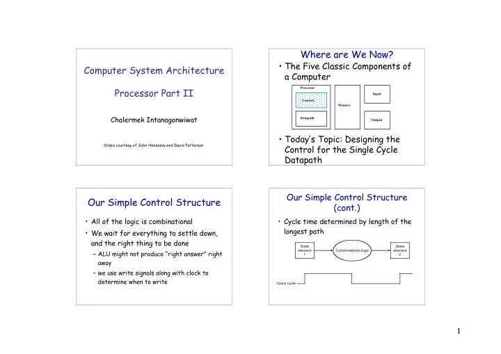
Where are We Now? The Five Classic Components of Computer System - - PowerPoint PPT Presentation

where are we now
SMART_READER_LITE
LIVE PREVIEW

Where are We Now? The Five Classic Components of Computer System - - PowerPoint PPT Presentation

Where are We Now? The Five Classic Components of Computer System Architecture a Computer Processor Part II Processor Input Control Memory Chalermek Intanagonwiwat Datapath Output Todays Topic: Designing the Slides courtesy of


slide-1
SLIDE 1

1

Computer System Architecture Processor Part II

Chalermek Intanagonwiwat

Slides courtesy of John Hennessy and David Patterson

Where are We Now?

  • The Five Classic Components of

a Computer

  • Today’s Topic: Designing the

Control for the Single Cycle Datapath

Control Datapath Memory Processor Input Output

  • All of the logic is combinational
  • We wait for everything to settle down,

and the right thing to be done

– ALU might not produce “right answer” right away – we use write signals along with clock to determine when to write

Our Simple Control Structure

  • Cycle time determined by length of the

longest path

Our Simple Control Structure (cont.)

Clock cycle State element 1 Combinational logic State element 2

slide-2
SLIDE 2

2

RTL: The Add Instruction

  • add

rd, rs, rt

– mem[PC] Fetch the instruction from memory – R[rd] <- R[rs] + R[rt] The actual

  • peration

– PC <- PC + 4 Calculate the next instruction’s address

  • p

rs rt rd shamt funct 6 11 16 21 26 31 6 bits 6 bits 5 bits 5 bits 5 bits 5 bits

Instruction Fetch Unit at the Beginning of Add

PC Ext

  • Fetch the instruction from

Instruction memory: Instruction <- mem[PC]

– This is the same for all instructions

Adr Inst Memory Adder Adder PC Clk 00 Mux 4 nPC_sel imm16 Instruction<31:0>

The Single Cycle Datapath during Add

32 ALUctr = Add Clk busW RegWr = 1 32 32 busA 32 busB 5 5 5 Rw Ra Rb 32 32-bit Registers Rs Rt Rt Rd RegDst = 1 Extender Mux Mux 32 16 imm16 ALUSrc = 0 ExtOp = x Mux MemtoReg = 0 Clk Data In WrEn 32 Adr Data Memory 32 MemWr = 0 ALU Instruction Fetch Unit Clk Zero Instruction<31:0> 1 1 1 <21:25> <16:20> <11:15> <0:15> Imm16 Rd Rs Rt nPC_sel= +4

Instruction Fetch Unit at the End

  • f Add
  • PC <- PC + 4

– This is the same for all instructions except: Branch and Jump

Adr Inst Memory Adder Adder PC Clk 00 Mux 4 nPC_sel imm16 Instruction<31:0>

slide-3
SLIDE 3

3

The Single Cycle Datapath during Or Immediate

32 ALUctr = Or Clk busW RegWr = 1 32 32 busA 32 busB 5 5 5 Rw Ra Rb 32 32-bit Registers Rs Rt Rt Rd RegDst = 0 Extender Mux Mux 32 16 imm16 ALUSrc = 1 ExtOp = 0 Mux MemtoReg = 0 Clk Data In WrEn 32 Adr Data Memory 32 MemWr = 0 ALU Instruction Fetch Unit Clk Zero Instruction<31:0> 1 1 1 <21:25> <16:20> <11:15> <0:15> Imm16 Rd Rs Rt nPC_sel= +4

The Single Cycle Datapath during Load

32 ALUctr = Add Clk busW RegWr = 1 32 32 busA 32 busB 5 5 5 Rw Ra Rb 32 32-bit Registers Rs Rt Rt Rd RegDst = 0 Extender Mux Mux 32 16 imm16 ALUSrc = 1 ExtOp = 1 Mux MemtoReg = 1 Clk Data In WrEn 32 Adr Data Memory 32 MemWr = 0 ALU Instruction Fetch Unit Clk Zero Instruction<31:0> 1 1 1 <21:25> <16:20> <11:15> <0:15> Imm16 Rd Rs Rt nPC_sel= +4

The Single Cycle Datapath during Store

32 ALUctr = Add Clk busW RegWr = 0 32 32 busA 32 busB 5 5 5 Rw Ra Rb 32 32-bit Registers Rs Rt Rt Rd RegDst = x Extender Mux Mux 32 16 imm16 ALUSrc = 1 ExtOp = 1 Mux MemtoReg = x Clk Data In WrEn 32 Adr Data Memory 32 MemWr = 1 ALU Instruction Fetch Unit Clk Zero Instruction<31:0> 1 1 1 <21:25> <16:20> <11:15> <0:15> Imm16 Rd Rs Rt nPC_sel= +4

The Single Cycle Datapath during Branch

32 ALUctr = Subtract Clk busW RegWr = 0 32 32 busA 32 busB 5 5 5 Rw Ra Rb 32 32-bit Registers Rs Rt Rt Rd RegDst = x Extender Mux Mux 32 16 imm16 ALUSrc = 0 ExtOp = x Mux MemtoReg = x Clk Data In WrEn 32 Adr Data Memory 32 MemWr = 0 ALU Instruction Fetch Unit Clk Zero Instruction<31:0> 1 1 1 <21:25> <16:20> <11:15> <0:15> Imm16 Rd Rs Rt nPC_sel= “Br”

slide-4
SLIDE 4

4

Instruction Fetch Unit at the End

  • f Branch
  • if (Zero == 1) then

PC = PC + 4 + SignExt[imm16]*4 ; else PC = PC + 4

Adr Inst Memory Adder Adder PC Clk 00 Mux 4 nPC_sel imm16 Instruction<31:0>

Step 4: Given Datapath: RTL -> Control

ALUctr RegDst ALUSrc ExtOp MemtoReg MemWr Equal Instruction<31:0> <21:25> <16:20> <11:15> <0:15> Imm16 Rd Rs Rt nPC_sel Adr Inst Memory DATA PATH Control Op <21:25> Fun RegWr

A Summary of Control Signals

inst Register Transfer ADD R[rd] <– R[rs] + R[rt]; PC <– PC + 4 ALUsrc = RegB, ALUctr = “add”, RegDst = rd, RegWr, nPC_sel = “+4” SUB R[rd] <– R[rs] – R[rt]; PC <– PC + 4 ALUsrc = RegB, ALUctr = “sub”, RegDst = rd, RegWr, nPC_sel = “+4” ORi R[rt] <– R[rs] | zero_ext(Imm16); PC <– PC + 4 ALUsrc = Im, Extop = “Z”, ALUctr = “or”, RegDst = rt, RegWr, nPC_sel = “+4”

A Summary of Control Signals (cont.)

LOAD R[rt] <– MEM[ R[rs] + sign_ext(Imm16)]; PC <– PC + 4 ALUsrc = Im, Extop = “Sn”, ALUctr = “add”, MemtoReg, RegDst = rt, RegWr, nPC_sel = “+4” STORE MEM[ R[rs] + sign_ext(Imm16)] <– R[rs]; PC <– PC + 4 ALUsrc = Im, Extop = “Sn”, ALUctr = “add”, MemWr, nPC_sel = “+4” BEQ if ( R[rs] == R[rt] ) then PC <– PC + sign_ext(Imm16)] || 00 else PC <– PC + 4 nPC_sel = “Br”, ALUctr = “sub”

slide-5
SLIDE 5

5

A Summary of the Control Signals (cont.)

add sub

  • ri

lw sw beq jump RegDst ALUSrc MemtoReg RegWrite MemWrite nPCsel Jump ExtOp ALUctr<2:0> 1 1 x Add 1 1 x Subtract 1 1 Or 1 1 1 1 Add x 1 x 1 1 Add x x 1 x Subtract x x x 1 x xxx func

  • p

00 0000 00 0000 00 1101 10 0011 10 1011 00 0100 00 0010 Appendix A 10 0000 See 10 0010 We Don’t Care :-)

The Concept of Local Decoding

R-type

  • ri

lw sw beq jump RegDst ALUSrc MemtoReg RegWrite MemWrite Branch Jump ExtOp ALUop<N:0> 1 1 x “R-type” 1 1 Or 1 1 1 1 Add x 1 x 1 1 Add x x 1 x Subtract x x x 1 x xxx

  • p

00 0000 00 1101 10 0011 10 1011 00 0100 00 0010 Main Control

  • p

6 ALU Control (Local) func N 6 ALUop ALUctr 3 ALU

The Encoding of ALUop

  • In this exercise, ALUop has to be 2 bits

wide to represent:

– (1) “R-type” instructions – “I-type” instructions that require the ALU to perform:

  • (2) Or, (3) Add, and (4) Subtract

Main Control

  • p

6 ALU Control (Local) func N 6 ALUop ALUctr 3

The Encoding of ALUop (cont.)

  • To implement the full MIPS ISA, ALUop

has to be 3 bits to represent:

– (1) “R-type” instructions – “I-type” instructions that require the ALU to perform:

  • (2) Or, (3) Add, (4) Subtract, and (5) And

(Example: andi)

R-type

  • ri

lw sw beq jump ALUop (Symbolic) “R-type” Or Add Add Subtract xxx ALUop<2:0> 1 00 0 10 0 00 0 00 0 01 xxx

slide-6
SLIDE 6

6

The Decoding of the “func” Field

R-type

  • ri

lw sw beq jump ALUop (Symbolic) “R-type” Or Add Add Subtract xxx ALUop<2:0> 1 00 0 10 0 00 0 00 0 01 xxx Main Control

  • p

6 ALU Control (Local) func N 6 ALUop ALUctr 3

  • p

rs rt rd shamt funct 6 11 16 21 26 31 R-type funct<5:0> Instruction Operation 10 0000 10 0010 10 0100 10 0101 10 1010 add subtract and

  • r

set-on-less-than ALUctr<2:0> ALU Operation 000 001 010 110 111 Add Subtract And Or Set-on-less-than Recall ALU Homework (also P. 286 text): ALUctr ALU

The Truth Table for ALUctr

R-type

  • ri

lw sw beq ALUop (Symbolic) “R-type” Or Add Add Subtract ALUop<2:0> 1 00 0 10 0 00 0 00 0 01 ALUop func bit<2> bit<1> bit<0> bit<2> bit<1> bit<0> bit<3> x x x x ALUctr ALU Operation Add 1 bit<2> bit<1> bit<0> x 1 x x x x Subtract 1 1 1 x x x x x Or 1 1 x x Add 1 1 x x 1 Subtract 1 1 1 x x 1 And 1 x x 1 1 Or 1 1 x x 1 1 Set on < 1 1 1 funct<3:0> Instruction Op. 0000 0010 0100 0101 1010 add subtract and

  • r

set-on-less-than

The Logic Equation for ALUctr<2>

  • ALUctr<2> = !ALUop<2> & ALUop<0> +

ALUop<2> & !func<2> & func<1> & !func<0>

ALUop func bit<2> bit<1> bit<0> bit<2> bit<1> bit<0> bit<3> ALUctr<2> x 1 x x x x 1 1 x x 1 1 1 x x 1 1 1 This makes func<3> a don’t care

The Logic Equation for ALUctr<1>

ALUop func bit<2> bit<1> bit<0> bit<2> bit<1> bit<0> bit<3> x x x x 1 ALUctr<1> x 1 x x x x 1 1 x x 1 1 x x 1 1 1 x x 1 1 1

  • ALUctr<1> = !ALUop<2> & !ALUop<1> +

ALUop<2> & !func<2> & !func<0>

slide-7
SLIDE 7

7

The Logic Equation for ALUctr<0>

ALUop func bit<2> bit<1> bit<0> bit<2> bit<1> bit<0> bit<3> ALUctr<0> 1 x x x x x 1 1 x x 1 1 1 1 x x 1 1 1

  • ALUctr<0> = !ALUop<2> & ALUop<0>

+ ALUop<2> & !func<3> & func<2> & !func<1> & func<0> + ALUop<2> & func<3> & !func<2> & func<1> & !func<0>

The ALU Control Block

ALU Contro l (Local) func 3 6 ALUop ALUctr 3

  • ALUctr<2> = !ALUop<2> & ALUop<0> +

ALUop<2> & !func<2> & func<1> & !func<0>

  • ALUctr<1> = !ALUop<2> & !ALUop<0> +

ALUop<2> & !func<2> & !func<0>

  • ALUctr<0> = !ALUop<2> & ALUop<0>

+ ALUop<2> & !func<3> & func<2> & !func<1> & func<0>

+ ALUop<2> & func<3> & !func<2> & func<1> & !func<0>

Step 5: Logic for each control signal

  • nPC_sel <= if (OP == BEQ) then

EQUAL else 0

  • ALUsrc <= if (OP == “Rtype”) then

“regB” else “immed”

  • ALUctr <= if (OP == “Rtype”) then

funct elseif (OP == ORi) then “OR” elseif (OP == BEQ) then “sub” else “add”

Step 5: Logic for each control signal (cont.)

  • ExtOp <= if (OP == ORi) then “zero”

else “sign”

  • MemWr <= (OP == Store)
  • MemtoReg

<= (OP == Load)

  • RegWr: <= if ((OP == Store) ||

(OP == BEQ)) then 0 else 1

  • RegDst: <= if ((OP == Load) ||

(OP == ORi)) then 0 else 1

slide-8
SLIDE 8

8

The “Truth Table” for the Main Control

R-type

  • ri

lw sw beq jump RegDst ALUSrc MemtoReg RegWrite MemWrite Branch Jump ExtOp ALUop (Symbolic) 1 1 x “R-type” 1 1 Or 1 1 1 1 Add x 1 x 1 1 Add x x 1 x Subtract x x x 1 x xxx

  • p

00 0000 00 1101 10 0011 10 1011 00 0100 00 0010 ALUop <2> 1 x ALUop <1> 1 x ALUop <0> 1 x Main Control

  • p

6 ALU Control (Local) func 3 6 ALUop ALUctr 3 RegDst ALUSrc

:

The “Truth Table” for RegWrite

R-type

  • ri

lw sw beq jump RegWrite 1 1 1

  • p

00 0000 00 1101 10 0011 10 1011 00 0100 00 0010

  • RegWrite = R-type + ori + lw

= !op<5> & !op<4> & !op<3> & !op<2> & !op<1> & !op<0> (R-type) + !op<5> & !op<4> & op<3> & op<2> & !op<1> &

  • p<0> (ori)

+ op<5> & !op<4> & !op<3> & !op<2> & op<1> &

  • p<0> (lw)

The “Truth Table” for RegWrite (cont.)

  • p<0>
  • p<5>. .
  • p<5>. .

<0>

  • p<5>. .

<0>

  • p<5>. .

<0>

  • p<5>. .

<0>

  • p<5>. .

<0> R-type

  • ri

lw sw beq jump RegWrite

PLA Implementation of the Main Control

  • p<0>
  • p<5>. .
  • p<5>. .

<0>

  • p<5>. .

<0>

  • p<5>. .

<0>

  • p<5>. .

<0>

  • p<5>. .

<0> R-type

  • ri

lw sw beq jump RegWrite ALUSrc MemtoReg MemWrite Branch Jump RegDst ExtOp ALUop<2> ALUop<1> ALUop<0>

slide-9
SLIDE 9

9

A Single Cycle Processor

32 ALUctr Clk busW RegWr 32 32 busA 32 busB 5 5 5 Rw Ra Rb 32 32-bit Registers Rs Rt Rt Rd RegDst Extender Mux Mux 32 16 imm16 ALUSrc ExtOp Mux MemtoReg Clk Data In WrEn 32 Adr Data Memory 32 MemWr ALU Instruction Fetch Unit Clk Zero Instruction<31:0> 1 1 1 <21:25> <16:20> <11:15> <0:15> Imm16 Rd Rs Rt Main Control

  • p

6 ALU Control func 6 3 ALUop ALUctr 3 RegDst ALUSrc

:

Instr<5:0> Instr<31:26> Instr<15:0> nPC_sel

Worst Case Timing (Load)

Clk PC Rs, Rt, Rd, Op, Func Clk-to-Q ALUctr Instruction Memoey Access Time Old Value New Value RegWr Old Value New Value Delay through Control Logic busA Register File Access Time Old Value New Value busB ALU Delay Old Value New Value Old Value New Value New Value Old Value ExtOp Old Value New Value ALUSrc Old Value New Value MemtoReg Old Value New Value Address Old Value New Value busW Old Value New Delay through Extender & Mux

Register Write Occurs

Data Memory Access Time

Drawback of Single Cycle CPU

  • Long cycle time:

– Cycle time must be long enough for the load instruction:

PC’s Clock -to-Q + Instruction Memory Access Time + Register File Access Time + ALU Delay (address calculation) + Data Memory Access Time + Register File Setup Time + Clock Skew

  • Cycle time for load is much longer than

needed for all other instructions

° Single cycle datapath => CPI=1, CCT => long ° 5 steps to design a processor

  • 1. Analyze instruction set => datapath requirements
  • 2. Select set of datapath components & establish clock methodology
  • 3. Assemble datapath meeting the requirements
  • 4. Analyze implementation of each instruction to determine setting of

control points that effects the register transfer.

  • 5. Assemble the control logic

° Control is the hard part ° MIPS makes control easier

  • Instructions same size
  • Source registers always in same place
  • Immediates same size, location
  • Operations always on registers/immediates

Summary

Control Datapath Memory Processor Input Output