ENHANCEMENT OF ETCHING FACTOR OF COPPER CIRCUIT BY CORRELATING - - PDF document

enhancement of etching factor of copper circuit by
SMART_READER_LITE
LIVE PREVIEW

ENHANCEMENT OF ETCHING FACTOR OF COPPER CIRCUIT BY CORRELATING - - PDF document

18 TH INTERNATIONAL CONFERENCE ON COMPOSITE MATERIALS ENHANCEMENT OF ETCHING FACTOR OF COPPER CIRCUIT BY CORRELATING BETWEEN MICROSTRUCTURE AND PATTERN SHAPE A. Hyo-Soo Lee 1 , B. Hai-Joong Lee 1 , C. Hyuk-Chon Kwon 1 1 Korea Institute of


slide-1
SLIDE 1

18TH INTERNATIONAL CONFERENCE ON COMPOSITE MATERIALS

Introduction Recently, small handheld electronic devices such as smartphone and tablet PC are a lightweight, extremely thin, short and feature prominently, the trend is improving. Thus, copper thin foil has been used as interconnection materials for various electronics as mobile, display and IT devices. As the electronics using GHz frequency and portable system have been increased, interconnection technology of printed circuit board and electronic package has also been important [1-2]. Especially, formation of finer pattern on printed circuit board affects multi-functions of final electronics such as device array, signal transmissibility and so on [3]. We have aimed at the established conditions for implementing a fine pitch of 35um or less that is possible in the semi-additive process as well as lowering the process price by using a subtractive process, which is a conventional mass-production

  • infrastructure. The pattern under 35um has been

known as possible only with the semi-additive process, which is cost-consumable process with high failure cost [4]. Accordingly in this study, we attempted to implement fine pattern formation by making crystal grains uniform through control of the fine structure of CCL and quantitatively analyze the etching ability according to fine structural change of

  • CCL. We investigated the relationship between

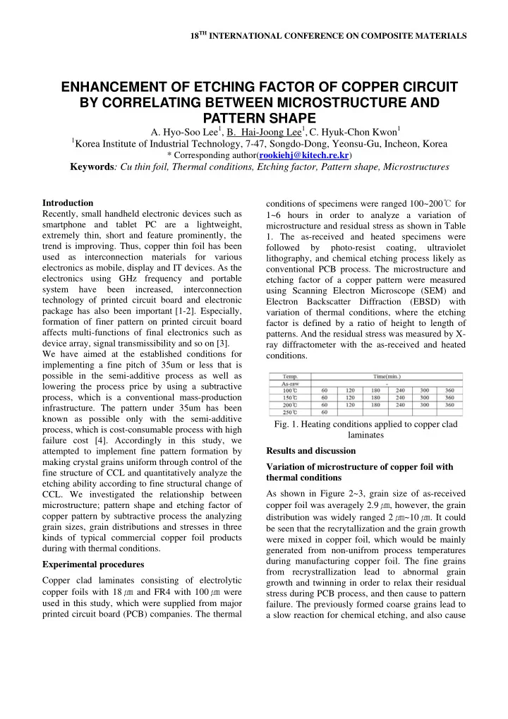
microstructure; pattern shape and etching factor of copper pattern by subtractive process the analyzing grain sizes, grain distributions and stresses in three kinds of typical commercial copper foil products during with thermal conditions. Experimental procedures Copper clad laminates consisting of electrolytic copper foils with 18 ㎛ and FR4 with 100 ㎛ were used in this study, which were supplied from major printed circuit board (PCB) companies. The thermal conditions of specimens were ranged 100~200℃ for 1~6 hours in order to analyze a variation of microstructure and residual stress as shown in Table

  • 1. The as-received and heated specimens were

followed by photo-resist coating, ultraviolet lithography, and chemical etching process likely as conventional PCB process. The microstructure and etching factor of a copper pattern were measured using Scanning Electron Microscope (SEM) and Electron Backscatter Diffraction (EBSD) with variation of thermal conditions, where the etching factor is defined by a ratio of height to length of

  • patterns. And the residual stress was measured by X-

ray diffractometer with the as-received and heated conditions.

  • Fig. 1. Heating conditions applied to copper clad

laminates Results and discussion Variation of microstructure of copper foil with thermal conditions As shown in Figure 2~3, grain size of as-received copper foil was averagely 2.9 ㎛, however, the grain distribution was widely ranged 2 ㎛~10 ㎛. It could be seen that the recrytallization and the grain growth were mixed in copper foil, which would be mainly generated from non-unifrom process temperatures during manufacturing copper foil. The fine grains from recrystrallization lead to abnormal grain growth and twinning in order to relax their residual stress during PCB process, and then cause to pattern

  • failure. The previously formed coarse grains lead to

a slow reaction for chemical etching, and also cause

ENHANCEMENT OF ETCHING FACTOR OF COPPER CIRCUIT BY CORRELATING BETWEEN MICROSTRUCTURE AND PATTERN SHAPE

  • A. Hyo-Soo Lee1, B. Hai-Joong Lee1, C. Hyuk-Chon Kwon1

1Korea Institute of Industrial Technology, 7-47, Songdo-Dong, Yeonsu-Gu, Incheon, Korea

* Corresponding author(rookiehj@kitech.re.kr)

Keywords: Cu thin foil, Thermal conditions, Etching factor, Pattern shape, Microstructures

slide-2
SLIDE 2

1 2 3 4 5 6 2.5 3.0 3.5 4.0 4.5 5.0 5.5

Mean grain size (μm)

100

  • C

150

  • C

200

  • C

250

  • C

to pattern failure. It is certainly sure that the non- uniform grain distribution and the residual stress are not good to form fine pattern using chemical etching process.

  • Fig. 2 Microstructure analysis of copper foil with

various thermal conditions

  • Fig. 3 Orientation Imaging Microscopy of copper

foil with thermal conditions

slide-3
SLIDE 3

3 PAPER TITLE

Copper clad laminates were applied by thermal conditions of 100~250 for 1~6 hours in order to ℃ improve grain distribution and to relax residual

  • stress. It was observed that grain size of as-received

copper foil of 2.9㎛ increased rapidly by 4.4 ~ 5㎛ durng heating at 100~250 for 1 hour, and grain ℃ size was increased slightly by 4.7~5.3㎛ during heating for 2~6hours. And also, when the heat treatment was conducted more than 1 hour, the standard deviation of grain size was decreased to 0.49, comparing with 1.01 of as-received copper foil, which demonstrated 50% improvement in uniformity of grain size during heating. Namely, the fine grains of as-received copper foil was increased to be coarse with heating temperature and time, which contributed to uniformity of grain size. It could be deemed that the grains of eletrolytic copper foil was easily changed even at the range of 100~ 250 and was controllable to form uniform ℃

  • microstructure. Heating at 250

gave rise to ℃ delamination between copper foil and FR4 due to a thermal damage of FR4, therefore, we could not

  • btained the whole data with heating times.
  • Fig. 4 Grain size distribution of copper foil with

thermal conditions. Table 1 and 2 are residual stress results by XRD. Also as shown in Figure 6, the variation of residual stress of electrolytic copper foil was measured with thermal conditions. The residual stress of as- received copper foil on CCL was evaluated as compressive stress of -53MPa. However, the compressive stress was relaxed to max. -12MPa with heating at 100~250℃ for 1 hour, which was correlated with uniformity of microstructure from a grain growth. And also the variation of residual stresses could be categorized phenomenologically into three regions as relaxed, constant, and compressive region with heating times.

  • Fig. 5 Measurement principle by residual stress
  • Fig. 6 Variation of residual stress of copper foil with

thermal conditions

slide-4
SLIDE 4

In the region I, the residual stresses of as- received copper foil were rapidly relaxed to max. - 12MPa, where the recrystalline grains were dominantly formed with relaxing the residual stress. Due to heterogeneous microstructure, compressed residual stress exists in the initial CCL. Therefore, increasing uniformity (of microstructure) and relaxing surface copper microstructure, residual stress was lost. In the region II, the residual stresses were nearly constant as - 34MPa, where the grain growth from recrystalline grains and from existent grains were mixed. As the results, the residual stresses were nearly steady. Residual stress maintenance section due to increasing uniformity (of microstructure) and relaxing surface copper

  • microstructure. In the region III, the residual stresses

were increased again as -36MPa ~ -55MPa, where the grain growth of all sites were dominantly

  • continued. The growth of grains in thin copper foils

causes to restrain growth of a neighbor copper grain, and consequently copper foils in region 3 is compressed again. Thermal stress and inherent stress

  • ccurrence due to long hours of heat treatment.

Contraction during cooling occurs due to hardening

  • f FR-4 layer. It could be known from these results

that the residual stresses of copper foil could be controlled with optimum temperature and time, where we expected to relate possibly residual stresses and etching factor. Especially, it is thougthful that the thermal conditions of the region II, nearly constant and lower residual stress, is more effective to increase a etching factor. The copper patterns were formed as line width, 100㎛ and spacing, 30㎛ with chemical etching process, where an as-received copper foil and an stress-relaxed copper foil heated at 100 ℃ for 2 hours were implanted in order to analyze etching factors with residual stresses as shown in Figure 7~8. The residual stress of as-received copper foil was -53MPa, which was very higher than that of stress-relaxed foil as -30MPa. The residual stresses

  • f copper foil influenced not only on the etching

factor but also on the pattern shape as shown Figure 8(a). It could be known that a rectangular shape pattern was formed with a decrease of residual stress. The formation of keen pattern was feasible by uniform grain distribution from relaxing residual

  • stress. The etching factors of copper foil were also

behaved with thermal conditions likely as the variation curves of residual stresses as shown in Figure 8(b). The etching factor of as-received copper foil was measured by 0.9, and increased to max. 1.4 with thermal conditions, which was very similar to the behavior of residual stresses as shown by dot line in Figure 8(b). It could be well understood that the etching factor was increased with decreasing the residual stress. And thus, we could suggest the good condition for chemical etching with uniform grain distribution and stress free.

  • Fig. 7 Cross section of copper foil with thermal

conditions

slide-5
SLIDE 5

5 PAPER TITLE

  • Fig. 8 Copper patterns and etching factor with

thermal conditions. (a) Comparison of etched patterns with thermal condition, (b) variation of etching factor with thermal conditions Summary It was analyzed in this study that the residual stresses were varied with thermal conditions, and could be categorized phenomenologically into three regions as relaxed, constant, and compressive region with heating times. Shape and etching factor of copper patterns were affected by the residual stresses due to uniform grains and relaxed stress, which gave the good conditions for chemical etching. As the residual stresses decreased, the etching factor was increased from 0.9 to 1.4 with a rectangular shape of copper pattern. It was expected to implement the formation of fine pattern by homogenizing grain sizes and by decreasing residual stress. References

[1] D. Edelstein J. Heidenreich, R. Goldblatt, W. Cote, C. Uzoh, N. Lustig, P. Roper, T. McDevitt, W. Motsifft,

  • A. Simon, J. Dukovic, R. Wachnik, H. Rathore, R.

Schulz, L. Su, S. Lucet and J. Slatteryt, Proc. IEEE- IEDM Conf., p.773 (1997). [2] J. Torres, Applied Surface Science 91, p.112~123 (1995) [3] R. L. Jackson, E. Broadbent, T. Cacouris, A. Harrus,

  • M. Biberger, E. Patton and T. Walsh, Solid State

Technology 41, 49 (1998). [4] Y. Morand, M. Lerme, J. Palleau, J, Torres, F, Vinet,

  • O. Demolliens, L. Ulmer, Y. Gobil, M. Fayolle, F.

Romagna and R. Le Bihan, Symposium on the VLST Technology Digest Technology Papers, p.31 (1997). [5] K. Ueno, K. Ohto and K. Tsunenari, Symposium on the VLST Technology Digest Technology Papers, p.27 (1995). [6] H-S Lee, H-J Lee, H-C Kwon, S-B Jung, The Microelectronics and Packaging Society, p.74(2009).