Basics of Digital Logic Design 0 1 1 0 1 0 0 1 1 1 0 1 0 - - PowerPoint PPT Presentation

basics of digital logic design
SMART_READER_LITE
LIVE PREVIEW

Basics of Digital Logic Design 0 1 1 0 1 0 0 1 1 1 0 1 0 - - PowerPoint PPT Presentation

Signals, Logic Operations and Gates CSE 675.02: Introduction to Computer Rather than referring to voltage levels of signals, we shall consider Architecture signals that are logically 1 or 0 (or asserted or de-asserted). Logic XOR NOT AND


slide-1
SLIDE 1

06-29-2005

Basics of Digital Logic Design

Presentation D CSE 675.02: Introduction to Computer Architecture

Gojko Babić

2

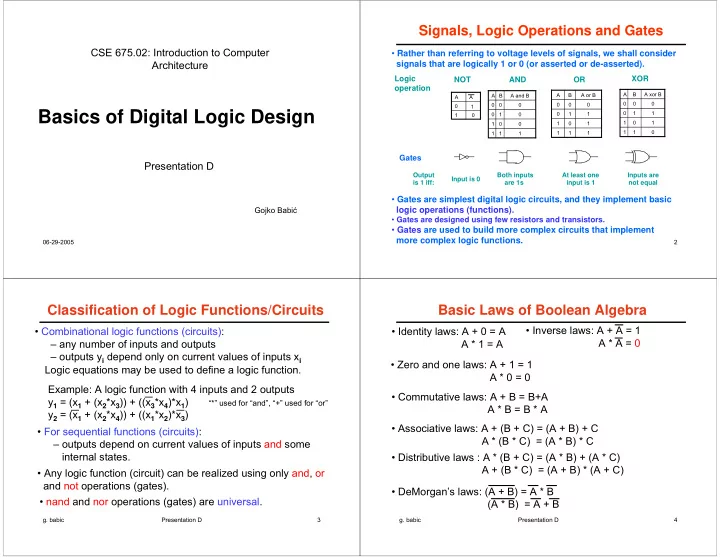
1 1 1 1 1 A and B B A 1 1 1 1 1 1 1 A or B B A

AND Logic

  • peration

XOR OR NOT

Output is 1 iff: Input is 0 Both inputs are 1s At least one input is 1 Inputs are not equal

1 A A 1 1 1 1 1 1 1 A xor B B A

Signals, Logic Operations and Gates

  • Rather than referring to voltage levels of signals, we shall consider

signals that are logically 1 or 0 (or asserted or de-asserted).

  • Gates are simplest digital logic circuits, and they implement basic

logic operations (functions).

  • Gates are designed using few resistors and transistors.
  • Gates are used to build more complex circuits that implement

more complex logic functions.

Gates

  • g. babic

Presentation D 3

Classification of Logic Functions/Circuits

  • Combinational logic functions (circuits):

– any number of inputs and outputs – outputs yi depend only on current values of inputs xi

  • For sequential functions (circuits):

– outputs depend on current values of inputs and some internal states.

  • Any logic function (circuit) can be realized using only and, or

and not operations (gates).

  • nand and nor operations (gates) are universal.

Example: A logic function with 4 inputs and 2 outputs y1 = (x1 + (x2*x3)) + ((x3*x4)*x1) “*” used for “and”, “+” used for “or” y2 = (x1 + (x2*x4)) + ((x1*x2)*x3) Logic equations may be used to define a logic function.

  • g. babic

Presentation D 4

Basic Laws of Boolean Algebra

  • Identity laws: A + 0 = A

A * 1 = A

  • Inverse laws: A + A = 1

A * A = 0

  • Zero and one laws: A + 1 = 1

A * 0 = 0

  • Commutative laws: A + B = B+A

A * B = B * A

  • Associative laws: A + (B + C) = (A + B) + C

A * (B * C) = (A * B) * C

  • Distributive laws : A * (B + C) = (A * B) + (A * C)

A + (B * C) = (A + B) * (A + C)

  • DeMorgan’s laws: (A + B) = A * B

(A * B) = A + B

slide-2
SLIDE 2
  • g. babic

Presentation D 5

Simple Circuit Design: Example

Given logic equations, it is easy to design a corresponding circuit y1 = (x1 + (x2*x3)) + ((x3*x4)*x1) = x1 + (x2*x3) + (x3*x4*x1) y2 = (x1 + (x2*x4)) + ((x1*x2)*x3) = x1 + (x2*x4) + (x1*x2*x3)

  • g. babic

Presentation D 6

Truth Tables

  • Another way (in addition to logic equations) to define certain

functionality

  • Problem: their sizes grow exponentially with number of inputs.

1 1 1 1 1 1 1 1 1 1 1 1 1 1 1 1 1 1 1 1

y2 y1 x3 x2 x1

inputs

  • utputs

What are logic equations corresponding to this table?

Design corresponding circuit.

y1 = x1 + x2 + x3 y2 = x1 * x2 * x3

  • g. babic

Presentation D 7

Logic Equations in Sum of Products Form

  • Systematic way to obtain logic equations from a given truth table.

1 1 1 1 1 1 1 1 1 1 1 1 1 1 1 1 1 1 1 1 1

y2 y1 x3 x2 x1

inputs

  • utputs
  • A product term is included for

each row where yi has value 1

  • A product term includes all input

variables.

  • At the end, all product terms are
  • red

+ x1*x2*x3 y1 = x1*x2*x3 + x1*x2*x3 + x1*x2*x3 + x1*x2*x3 y2 = x1*x2*x3 + x1*x2*x3 + x1*x2*x3 + x1*x2*x3

  • g. babic

Presentation D 8

AND gates OR gates Product terms Outputs Inputs

Programmable Logic Array - PLA

  • PLA – structured logic implementation
slide-3
SLIDE 3
  • g. babic

Presentation D 9

Circuit Logic Equation Truth Table

  • For the given logic circuit find its logic equation and truth table.

+ x2*x3 y = x1*x2

1 1 1 1 1 1 1 1 1 1 1 1 1 1 1 1

y x3 x2 x1

  • Note that y column above is identical to y1 column Slide 7.
  • Thus, the given logic function may be defined with different

logic equations and then designed by different circuits.

x1 x3 x2 y

  • g. babic

Presentation D 10

Minimization Applying Boolean Laws

+ x1*x2*x3 y1 = x1*x2*x3 + x1*x2*x3 + x1*x2*x3

  • Consider one of previous logic equations:

= x1*x2*(x3 + x3) + x2*x3*(x1 + x1) = x1*x2 + x2*x3

But if we start grouping in some other way we may not end up with the minimal equation.

  • g. babic

Presentation D 11

Minimization Using Karnough Maps (1/4)

  • Provides more formal way to minimization
  • Includes 3 steps
  • 1. Form Karnough maps from the given truth table. There is one

Karnough map for each output variable.

  • 2. Group all 1s into as few groups as possible with groups as

large as possible.

  • 3. each group makes one term of a minimal logic equation for the

given output variable.

Forming Karnough maps

  • The key idea in the forming the map is that horizontally and vertically

adjacent squares correspond to input variables that differ in one variable only. Thus, a value for the first column (row) can be arbitrary, but labeling of adjacent columns (rows) should be such that those values differ in the value of only one variable.

  • g. babic

Presentation D 12

Minimization Using Karnough Maps (2/4)

Grouping (This step is critical)

When two adjacent squares contain 1s, they indicate the possibility of an algebraic simplification and they may be combined in one group of

  • two. Similarly, two adjacent pairs of 1s may be combined to form a group
  • f four, then two adjacent groups of four can be combined to form a

group of eight, and so on. In general, the number of squares in any valid group must be equal to 2k. Note that one 1 can be a member of more than one group and keep in mind that you should end up with as few as possible groups which are as large as possible. The product term that corresponds to a given group is the product of variables whose values are constant in the group. If the value of input variable xi is 0 for the group, then xi is entered in the product, while if xi has value 1 for the group, then xi is entered in the product.

Finding Product Terms

slide-4
SLIDE 4
  • g. babic

Presentation D 13

+ x2*x3 y = x1*x2

Minimization Using Karnough Maps (3/4)

1 1 1 1 00 01 11 10 1 x1 x2 x3 1 1 1 1 1 1 1 1 1 1 1 1 1 1 1 1

y x3 x2 x1

Example 1: Given truth table, find minimal circuit

Presentation D 14

Minimization Using Karnough Maps (4/4)

Example 2:

y = x1*x3 + x2

1 1 1 1 1 00 01 11 10 00 01 11 10 x1x2 x3x4 1 1 1 1 1 1 1 00 01 11 10 00 01 11 10 x1x2 x3x4

Example 3: Example 4: y = x1*x2*x3 + x1*x2*x4 + x2*x3*x4 y = x1*x4 + x2*x3*x4 + x1*x2*x3*x4

x1 x2 1 1 1 1 1 00 01 11 10 1 x3

  • g. babic

Presentation D 15

Decoders

  • A full decoder with n input has 2n outputs. Let inputs be labeled

In0, In1, In2,..., Inn-1, and let outputs be labeled Out0, Out1,..., Out2n-1.

  • A full decoder functions as follows: Only one of outputs has

value 1 (it is active) while all other outputs have value 0. The

  • nly output set to 1 is one labeled with the decimal value equal

to the (binary) value on input lines.

  • In general, a decoder with n inputs may have fewer than 2n
  • utputs. Sometime those are called partial decoders. Decoders

with only one output are common.

  • g. babic

Presentation D 16

Out0 Out1 Out2 Out3 Out4 Out5 Out6 Out7 Decoder 3

3-Input Full Decoder

1 1 1 1 1 1 1 1 1 1 1 1 1 1 1 1 1 1 1 1 O0 O1 O2 O3 O4 O5 O6 O7 I0 I1 I2

Input Output

slide-5
SLIDE 5
  • g. babic

Presentation D 17

Multiplexers

  • A basic multiplexer has only one output line z. There are two

sets of input lines: data lines and select lines.

  • Let a number of data lines be N, labeled d0, d1, d2,... dN-1. There

are m select lines, labeled s0, s1,..., sm-1. m is such that any of data lines can be referenced (selected) by a decimal value on select lines. Thus, m has to satisfy the following inequality: 2m-1 < N ≤ 2m.

  • A multiplexer functions as follows: Output z has the value of

the data input line labeled by a decimal value equal to a (binary) value on select lines.

  • g. babic

Presentation D 18

C A B S 1 A C B S M u x

Simplest Basic Multiplexer

1 1 1 1 1 1 1 1 1 1 1 1 1 1 1 1 C S B A

Symbol Truth Table Design (just using right thinking)

Simplest mux is one with 2 data input lines and 1 select line.

  • g. babic

Presentation D 19

3-Data Multiplexer Truth Table

do d1 d2 s1 s0 z 0 0 0 0 0 0 0 0 0 0 1 0 0 0 0 1 1 d 0 0 0 1 0 0 0 0 1 0 0 0 0 0 1 0 1 0 0 0 1 1 0 1 0 0 1 1 1 d 0 1 0 0 0 0 0 1 0 0 1 1 0 1 0 1 0 0 0 1 0 1 1 d 0 1 1 0 0 0

  • 1 1 1 1 0 1

1 1 1 1 1 d

This input not allowed This input not allowed This input not allowed

  • g. babic

Presentation D 20

M u x S e l e c t 3 2 A 3 2 B 3 2 C M u x S e l e c t A 3 1 B 3 1 C 3 1 M u x A 3 0 B 3 C 3 M u x A B C

Complex Multiplexer

  • Instead N single data lines and one output line as in a basic

mux, a complex mux has N sets of data lines and one set of

  • utput lines and each set has K lines.
  • No changes with select lines.

N=2, K=32

1 1 1 1

Design mux

  • n left at

basic mux level

slide-6
SLIDE 6
  • g. babic

Presentation D 21

R-S Latch: Simplest Sequential Circuit

1 1 1 1 1 A nor B B A

R S Qa Qb

  • 1. Let us start with: S = 0 & R = 1

Qa = 0 & Qb = 1 1 1 1

  • 2. Let us now change R to 0: S = 0 & R = 0

Qa = 0 & Qb = 1, i.e. no change

  • 3. Let us now change S to 1: S = 1 & R = 0

1 1 Qa = 1 & Qb = 0

  • 4. Let us now change S to 0: S = 0 & R = 0

Qa = 1 & Qb = 0, i.e. no change

Thus, for steps 2 and 4 inputs are identical while outputs are different, i.e. we have a sequential circuit.

1

  • g. babic

Presentation D 22

R-S letch is a memory element that “remembers” which of two inputs has most recently had value 1:

R-S Latch Characteristics

  • Outputs Qa =1 & Qb = 0 indicate that S is currently or was 1 last
  • Outputs Qa =0 & Qb = 1 indicate that R is currently or was 1 last

R S Qa Qb

  • g. babic

Presentation D 23

R-S Latch Characteristics (continued)

1 1 1 1 1 A nor B B A

R S Qa Qb

  • 5. Let us consider case: S = 1 & R = 1

Qa = 0 & Qb = 0 1

  • 6a. Let us now change S to 0: S = 0 & R = 1 Qa = 0 & Qb = 1,

Identical to Step 1 on Slide 21

Qa = 0 & Qb = 0 indicate currently S = 1 and R = 1

1 1 1

  • g. babic

Presentation D 24

R-S Latch Characteristics (continued)

1 1 1 1 1 A nor B B A

R S Qa Qb

  • 5. Let us again consider case: S = 1 & R = 1

Qa = 0 & Qb = 0 1

  • 6b. Let us now change S and R simultaneously to 0: S = 0 & R = 0

1 1 1 1 1 Unstable state

Note: This scenario may be interesting, but it is not that important.

slide-7
SLIDE 7
  • g. babic

Presentation D 25

Gated R-S Latch

R S Qa Qb

  • C input is write enable (not a clock)
  • When C = 1, a gated R-S latch behaves as an ordinary

R-S latch.

  • When C = 0, changes in R and S do not influence outputs.
  • Note that the case R’=1 & S’=1 is still possible, and the

unstable state can be reached easily. How?

R S C ‘ ‘

  • g. babic

Presentation D 26

  • Two inputs:

– the data value to be stored (D) – the write enable signal (C) indicating when to read & store D

  • Two outputs:

– the value of the internal state (Q) and it's complement (often unused)

  • Note: The case R’=1 & S’=1 is not possible.

(Gated) D-Latch

Q C D _ Q

R’ S’

  • g. babic

Presentation D 27

  • D-latch functions as follows:

– when C=1, D-latch state (and Q-output) is identical to D- input, i.e. any change in the value of D-input is immediately followed by the change of Q-output. – When C=0, D-latch state is unchanged and it keeps the value it had at the time when C input changed from 1 to 0.

D-Latch Functioning

Q C D _ Q

D latch

D C Q

  • g. babic

Presentation D 28 Q Q _ Q Q _ Q D latch D C D latch D D C C

D Flip-Flop

  • Two inputs:

– the data value to be stored (D) – the write enable signal (C) indicating when to read & store D

  • Two outputs:

– the value of the internal state (Q) and it's complement (often unused)

D flip-flop

D C Q

D flip-flop inputs and Outputs identical to that Of D-latch.

slide-8
SLIDE 8
  • g. babic

Presentation D 29 Q Q _ Q Q _ Q D latch D C D latch D D C C

D Flip-Flop Functioning

  • D-flip-flop functions as follows:

– When C changes its value from 1 to 0, i.e. on the falling edge, D-flip flop state (and Q output) gets the value D-input has at that moment, – During all other times, D-flip flop state is unchanged and it keeps the value it had at the time of the falling edge of C-input.

  • There is is critical period Tcr around the falling edge of C during wich

value on D should not change. Tcr is split into two parts, the setup time before the C edge, and the hold time after the C edge.

1 1 1 1 1 1 1

  • g. babic

Presentation D 30

Three State D-Latch

  • Three inputs:

– the data value to be stored (D) – the write enable signal (C) indicating when to read & store D – the read enable signal (E) indicating when internal state is provided

  • n the output
  • One output:

– the value of the internal state (Q) ??

Q C D E

D latch

D C Q E Presentation D 31

Three State D-Latch Functioning

  • Storing (writing) is performed as in the case of the (ordinary) D-

latch)

  • When E=1 (enable read), then the switch is closed,

and Q has value (0 or 1) that has been stored (written) into the D-latch

  • When E=0 (disable read), then the switch is open,

and Q is in the high impendence state (the third possible “value” on the output).

Q C D E

  • g. babic

Presentation D 32

32-bit Register Design

  • D flip-flop as a building block

D flip-flop

D C Q

D flip-flop D flip-flop D flip-flop D flip-flop

. . .

1 2 30 31 Dout Dout Dout Dout Dout Din0 Din1 Din2 Din30 Din31 Write

  • Thus, 32-bit register has:

– 33 inputs and – 32 outputs

  • There are two operations on

a register: – read and – write

  • Read operation:

– register content is always available on Dout0-Dout31

  • Write operation:

– provide desired values on Din0-Din31 – generate falling edge on the write line – Recall critical period Tcr around falling edge.